Europe has become an area where special IC´s and electronic applications are being developed and produced, such as Sensors, MEMS, vision applications, specific IC’s, etcetera, in particular for semiconductor, automotive and medical applications.In 2004 TOWA Europe GmbH was established, to serve the many European customers. The activities originally consisted of the supply of the TOWA encapsulation equipment, after sales service and spare parts.
However, in addition to this, the cooperation with the package/product development centers of European customers and European institutes became an important activity and TOWA Europe started to play a leading role in the development of new products.
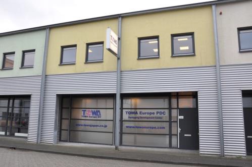
To further expand this, it has been decided to establish a Packaging Development Center in the Netherlands, for which TOWA Europe has been founded. This center is located at Geograaf 14, Duiven, The Netherlands.
Laboratory
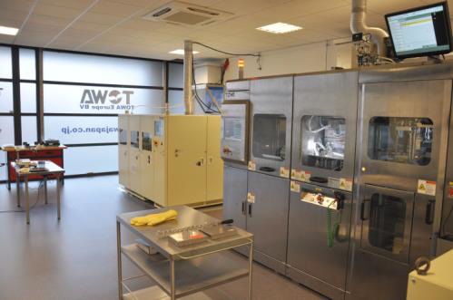
 A fully equipped laboratory with 2 TOWA molding systems, test and measuring equipment as well as an engineering department is available to give full support in all the phases of product development, from initial concept up to test, qualification and industrialization. The Dutch, German and English speaking staff will be happy to assist European customers with the exciting process of new package development. Also the European Marketing, Sales and Service department for the TOWA systems is located at this new facility.
About TOWA
The TOWA Corporation of Japan, founded in 1979, is a leading supplier of molding and singulation equipment for the global semiconductor and electronics industries.
The Company develops molding processes and equipment for leadframe, substrate, large panels and wafer level packaging. Applications in a wide range of end-user markets including electronics, computer, automotive, industrial, RFID, LED and solar energy. The transfer molding and compression molding technology, developed by TOWA, has become the leading technology in the fields of Semiconductor & Electronics Packaging and LED lens manufacturing. Customers are leading semiconductor manufacturers, assembly subcontractors and electronics and industrial companies.
TOWA Europe B.V. is a fully owned subsidiary of the TOWA Corporation of Japan and is located at Geograaf 14, 6921 EW Duiven, the Netherlands.


