| The 2012 update of the SSL Manufacturing R&D Roadmap guides research programs in LED and OLED manufacturing with the goal of meeting aggressive cost targets for 2015 and 2020.
| |
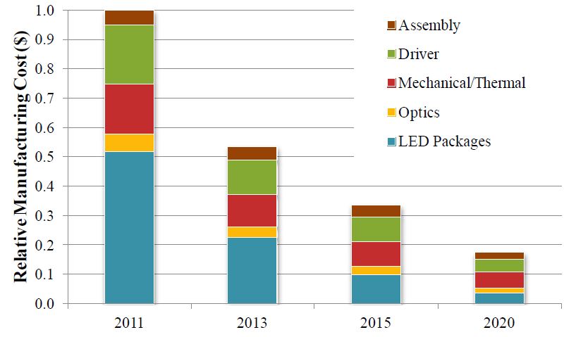
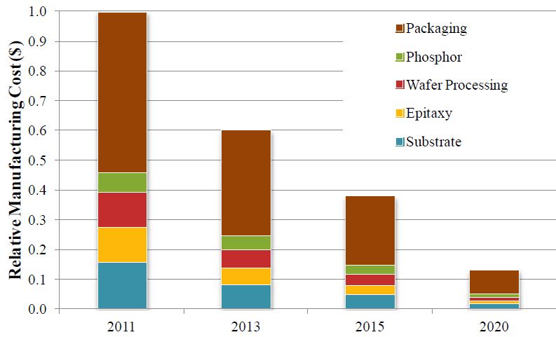
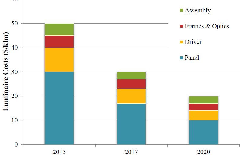
| The US Department of Energy (DOE) has published the 2012 edition of the Solid-State Lighting (SSL) Manufacturing R&D Roadmap. This update is the result of recommendations made at the April meetings of OLED and LED expert panels as well as work performed by 200 attendees at the 4th annual SSL Manufacturing R&D Workshop, held in San Jose, CA on June 13–14. The workshop report can be accessed at the link above. The Roadmap's primary goal is to direct funding solicitations for the manufacturing R&D program and it complements the DOE SSL R&D Multi-Year Program Plan (MYPP) that guides the Core and Product Development R&D programs. The Roadmap also provides guidance for equipment and material suppliers based on industry consensus on the expected evolution of SSL manufacturing - thereby reducing risk, improving product quality, increasing yields, and lowering costs. FIG.1 Manufacturing tool developments At the workshop, attendees were provided with an update of DOE-funded projects involving many companies including Universal Display Corp (UDC), Moser Baer, Applied Materials, Veeco, Sandia National Labs, KLA-Tencor, GE Lighting Solutions, Ultratech, Philips Lumileds and DuPont Displays. Ultratech has optimized its Sapphire 100 projection lithography tool for LED manufacturing. The goal was to make the equipment compatible with the wide range of substrate diameters and thicknesses used in the industry while reducing capital cost and cost-of-ownership (COO). In a side-by-side comparison with a conventional contact lithography system in a commercial fabrication facility, the Ultratech tool demonstrated yield and throughput advantages. Applied Materials is developing a sequential 3-chamber process that combines MOCVD with hybrid vapor phase epitaxy (HVPE), a faster and less expensive deposition technique for thin films. This combination is designed to decrease overall operating cost, and increase internal quantum efficiency, and improve binning yields. GE Lighting Solutions has developed a phosphor material that is combined with a polymer carrier to make it injection moldable. This allows remote phosphor components to utilize a reduced phosphor content (75-80% less than previous formulations). Using blue LEDs and the remote phosphor component, GE has made warm-white light with a color shift of less than 1 MacAdam step after 6000 hours, better performance than with phosphor-on-chip. Veeco Instruments worked with Philips Lumileds and Sandia National Labs to reduce the COO of its Maxbright MOCVD system. A new wafer carrier with special pocket shaping has enabled significant improvements in wavelength uniformity. Sandia has developed process modeling software using computational fluid dynamics to optimize MOCVD process efficiency. Overall, COO has been reduced 66%. DuPont Displays has developed a method of printing color-tunable OLED lighting panels based on low-cost manufacturing processes. A group of 50 cm2 prototypes were incorporated into task-lighting luminaires that were tunable from a CCT of 2700K to 6500K. Panels achieved an efficacy of 35 lm/W at 2700K. Key LED targets The LED expert panel identified four priority tasks for LEDs including support for the development of flexible manufacturing of state-of-the-art modules, light engines, and luminaires; development of high-speed, nondestructive test equipment and metrics for each stage of production; identification of critical issues with back-end processes for packaged LEDs; and improved manufacturing of phosphors or other down-converters. The roadmap states that suitable development activities for the luminaire/module would fall into one or more of the following areas: 1. Advanced LED package and die integration (e.g. chip-on-board, chip-on-foil, etc.) into the luminaire, Specific targets for 2015 include a 2X increase in throughput, reduction in OEM lamp price from $50/klm to $10/klm, 50% reduction in assembly cost every 2-3 years and color control improvement from 7 SDCM to 4 SDCM. FIG.2 The roundtable discussion of LED packaging manufacturing revolved around using lower cost materials and manufacturing processes within the LED package. Specifically, by 2012 it calls for a 2X increased in packaged LED throughput each year, 50% reduction is assembly cost/klm every 2-3 years, 50% reduction in the cost of packaging ($/mm2) every 2-3 years and a 50% reduction in the cost per package ($/klm) every 2-3 years.The test and inspection discussion called for support for the development of high-speed, high-resolution, non-destructive test equipment with standardized test procedures and appropriate metrics within each stage of the value chain - for semiconductor wafers, epitaxial layers, LED die, packaged LEDs, modules, luminaires, and optical components. Equipment might be used for incoming product quality assurance, in-situ process monitoring, in-line process control, or final product testing/binning. Specific target metrics for testing and inspection by 2015 include a doubling of throughput in single bin units/hr, and a 2-3X reduction in COO every 5 years. One specific area of interest involves the high-speed monitoring of light output, color quality, and color consistency at the wafer level at LED operating temperature. Such test equipment would facilitate the automation of LED and phosphor matching and accelerate final device binning. Regarding improved manufacturing of phosphors, by 2015 the roadmap calls for larger batch sizes (from 1-5 kg to 20 kg), a 50% reduction in the cost/kg every 2-3 years, raising the phosphor utilization from 50% to 90%, improving the PSD range uniformity from 30 to 10, improving Duv control from 0.012 to <0.002, improving thickness uniformity from 5% (1 sigma) to 2% (1 sigma), reducing cost/klm by 50% and improving device-to-device reproducibility of 4 SDCM to 2 SDCM. One of the more significant changes to the 2012 document is the emphasis on manufacturing cost reduction rather than price reduction. Therefore, it is critical when examining the charts such as the manufacturing cost of an LED-based A19 60W lamp (Fig. 1), which is based purely on manufacturing costs, that it not be confused with data that tracks the packaged LED cost (Fig. 2) and does include gross margin, and is therefore more legitimately referred to as a price. Key OLED targets Based on necessary spending cuts, the OLED expert panel decided to narrow the focus from three priority tasks last year to two tasks this year. The priorities involve developing improved OLED deposition equipment and better OLED materials. The roadmap calls for the development of OLED manufacturing equipment that enables high speed, low cost, and uniform deposition of state-of-the-art OLED structures and layers. The cost target is <$100 per square meter of good panel produced. FIG.3 On the materials side, both substrate and encapsulation materials must meet stringent specifications by 2015. These include a substrate extraction efficiency of 50%, sheet resistance of <1 ohm/sq, and total cost of $60/m2. The encapsulation material must pass a water permeability spec of 10-6 g/m2/day, oxygen permeability of 10-4 cc/m2/day/atm and cost of $35/m2. The current price of OLED luminaire samples is $1500-2000/klm and Philips has indicated that panels can be purchased in the $800/klm range. The 2012 Roadmap assumes that by 2015, OLED R&D lines will be converted to production lines and the OLED luminaire cost can be brought to $50/klm while OLED panel cost will be $30/klm (Fig. 3). The targets for 2015 are based on estimates by Moser Baer, whose strategy is to minimize cycle time while using relatively small substrates. The roadmap lists the most critical short-term challenges as:
Overall, OLED production cost needs to be reduced by 20-100X to make OLEDs competitive with, for instance, edge-lit LED luminaires that produce diffuse light. |


