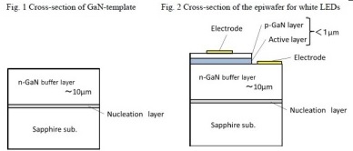
Hitachi Cable has launched a new mass-production technology for GaN-templates as shown in Figures 1 and 2 below.

The process allows high-quality GaN single-crystal thin film to be grown on a sapphire substrate and the company plans to start selling these templates.
Using this product as a base substrate for an epitaxial wafer for white LEDs the company claims it makes it possible to drastically improve productivity of white LED epiwafers and the LED properties.
Therefore, this product is expected to become an effective solution to improve the position of white LED manufacturers in the industry, where there is severe competition.
The demand for white LEDs is rapidly expanding and they have come to be used in backlight unit in LCDs and ordinary lighting devices in recent years thanks to their energy efficiency and long service life.
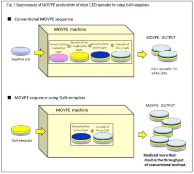
The structure of an white LED epiwafer consists of a thin active layer and a p-type GaN layer with a total thickness of about 1μm over an n-type GaN layer with a thickness of about 10μm, grown on a sapphire substrate as shown in Figure 3 below.

All these crystal layers are produced by the MOVPE processes. The MOVPE method is suitable for growing active layers which require atomic-level control of the film thickness.
Meanwhile, a disadvantage of this method is that it takes a long time to grow a high-quality and thick n-type GaN layer. White LED epiwafers can be grown about once or twice a day at the most, and thus there is a need for a high-efficiency production method.
To solve this problem, Hitachi Cable developed a GaN-template used as a base substrate for growth in the MOVPE method.
The GaN template consists of an n-type GaN layer grown on a sapphire substrate. Using a GaN-template means LED manufacturers do not need to grow an n-type GaN buffer layer and this reduces the time required for growth by about half compared with conventional methods.
Hitachi Cable says its GaN-templates are also suitable for high-output LEDs which require large currents because they allow both low resistance and high crystal formation.
The firm has developed single-crystal free-standing GaN substrates used for blue-violet lasers and developed unique HVPE-growth technology and machines for mass-production of GaN substrates.
Based on this technology, Hitachi Cable developed new high-efficiency production technology and machines for mass-production of high-quality GaN-templates.
The main characteristics of the GaN-template are as follows.
High crystal quality and high surface quality based on growth technology established in the development of free-standing GaN substrates
Low resistance n-type GaN buffer which is suitable for high-output wafers and bonding-type LEDs
Templates on flat-surface sapphire substrates and various types of PSS are available
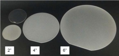
Wafers with 2 to 6 inches in diameters are available, with an 8-inch version now planned for developmen). Photos of the substrates currently avalable are shown below.

Panel exhibits of GaN-templates will be presented at CS Mantech which will be held in New Orleans in the United States from May 13th to 16th.


