After recovering strongly from 2009 with growth of 22% in 2010, the gallium arsenide (GaAs) substrate market slowed sharply in 2011, rising just 4% to nearly $360m, due to weak demand in RF circuits (handsets and WLANs) and in optoelectronics (LEDs and laser diodes), according to market research firm Yole Développement in its report ‘GaAs Wafer Market & Applications’.
However, the market is expected to recover in 2012, driven by (i) the sheer volume of the handset market and (ii) consolidation of the LED industry (balance of capacity).
The GaAs substrate market should hence increase at a compound annual growth rate (CAGR) of nearly 11% to more than $650m by 2017 (Figure 1), fuelled primarily by: rising GaAs content in handsets; and rising penetration of LEDs in general lighting and automotive applications.

Figure 1: GaAs wafer market trend.
RF electronics (power amplifiers, switches etc) initially comprised the main market for GaAs wafers and will continue to fuel the business in the coming years due to the development of sophisticated smartphones, the development of 3G/4G networks, and the increased demand for data communications, says Yole.
But recently the development of new GaAs-based devices is boosting the market with associated high-volume applications (e.g. LEDs, which are currently booming due to their advantages over traditional light sources). Other devices such as solar cells for high-concentration photovoltaics (HCPV) will also add to the development of the GaAs substrate market, but to a lesser degree, reckons Yole.
Boosted by LEDs, semiconducting GaAs substrates to lead growth
In 2011, the semi-insulating (SI) GaAs substrate market represented about 56% of the overall GaAs substrate market by value, versus 44% for semi-conducting (SC) GaAs. However, this trend is likely to reverse in the short term, as GaAs substrate demand for LEDs should rapidly surpass demand for RF electronics devices (Figure 2).

Figure 2: Market share ($m) of SI GaAs and SC GaAs (2011 and 2017).
Globally, the penetration rate of LEDs is increasing in applications including TVs, signs & displays etc. Also, if fundamental technology improvements are achieved to improve LED efficiency and increase the total amount of light generated per package, then general lighting should be the next ‘killer application’, boost the SC GaAs substrate market in 2012-2013. Moreover, the automotive industry is also shifting from the use of traditional light sources to LEDs for products such as headlamps and interior lights.
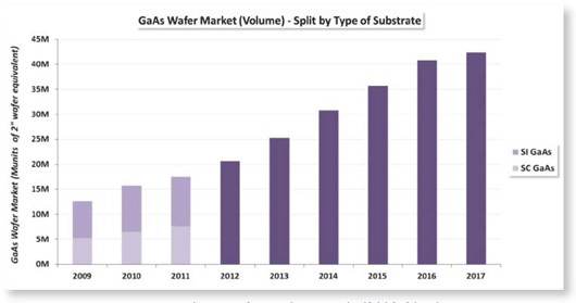
In that context, SC GaAs substrate volumes are likely to equal SI GaAs substrate volumes by 2013 due to steady growth in the RF electronics market compared to booming growth in the optoelectronics market.
Earthquake in 2011 shifted revenue of some Japanese players to competitors
The Japanese earthquake/tsunami in 2011 damaged several manufacturing plants and strongly impacted the production capacity of some key GaAs substrate suppliers, who lost market share to competitors (Figure 3).

Figure 3: GaAs wafer market ($m), split by players (2010 and 2011).
Whether these companies will invest to recover operations, reduce operations or exit the business is still unclear, says Yole. However, the GaAs wafer industry is evolving and some players have already announced plant expansion in order to gain market share and prepare future growth of the market, the market research firm notes.
At this level, due to its lower labor cost, China seems to be the new ‘El Dorado’ of GaAs wafer manufacturing: all expansions plans announced will be localized in the country, Yole reckons.


