Researchers in the USA have reduced current leakage for aluminium gallium nitride (AlGaN) high-electron-mobility transistors (HEMTs) on silicon to the level achieved for devices produced on much more expensive silicon carbide [Bo Song et al, IEEE Electron Device Letters, published online 3 November 2015].
The team from Cornell University, University of Notre Dame and IQE Massachusetts used re-grown source/drain contacts that avoided alloying processes to reduce contact resistance. The researchers comment: "HEMTs with non-alloyed contacts avoid unfavorable high-temperature processes, thus effectively suppressing the leakage commonly observed in AlGaN HEMTs."
Such HEMTs are being developed for high-speed high-power radio-frequency electronics, along with high-power conversion and switching.
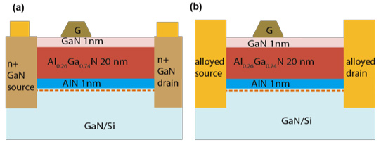
Figure 1: Schematic cross section of AlGaN/GaN HEMT on silicon with (a) non-alloyed contacts re-grown by MBE and (b) alloyed contacts.
The epitaxial material structures for the HEMTs (Figure 1) were grown on 6-inch (150mm) silicon using metal-organic chemical vapor deposition (MOCVD). The GaN buffer was 1.3μm thick.
The non-alloyed contacts were created with 660°C molecular beam epitaxy (MBE) of heavily doped n-type GaN. The re-growth regions for the n+-GaN were made by reactive ion etch to a depth of 40nm through a silicon dioxide mask. The re-growth material was 80nm thick. The ohmic contact metals were titanium/gold.
Alloyed-contact comparison devices were produced with a titanium/aluminium/nickel/gold stack annealed in nitrogen at 870°C for 20 seconds.
The specific contact resistances of the re-grown and alloyed contacts were 0.1Ω-mm and 0.3Ω-mm, respectively. Hall measurements gave respective two-dimensional electron gas (2DEG) concentrations of 7.63x10¹²/cm2 and 4.57x10¹²/cm2. The corresponding mobilities were 1620cm2/V-s and 1420cm2/V-s.
The HEMT devices had 2μm-long, 50μm-wide nickel/gold gates. The gate-drain/gate-source spacings were 4.75μm/2μm. No passivation was used.
The output drain current at 1V gate and 6V drain bias was 0.42A/mm for the non-alloyed re-grown contact and 0.29A/mm for the alloyed device. The respective peak transconductances were 142mS/mm and 126mS/mm. The corresponding threshold voltages were -2V and -1.4V, putting both devices firmly in the normally-on/depletion-mode camp.
The off-state gate leakage was ~10-12A/mm for the non-alloyed/re-grown HEMT. The corresponding leakage for the alloyed device was ~10-6A/mm. The researchers comment that the non-alloyed HEMT is close to the record low for GaN HEMTs produced on any substrate (e.g. expensive silicon carbide).
The subthreshold slope was also reduced in the non-alloyed HEMT – 73mV/decade, compared with 166mA/decade for the alloyed device. The theoretical limit at 300K is around 60mV/decade. The on/off current ratio is given as 2.5x10¹¹ for the non-alloyed HEMT and 1.1x10⁵ for the alloyed device.
Soft breakdown for the alloyed HEMT occurred around 100V at 100μA/mm (10-4A/mm), compared with the non-alloyed/re-grown contact device maintaining a low leakage at less than 10-10A/mm up to 156V. The increase in current after 156V bias was attributed to field crowding near the gate edge. Neither of the devices employed field plates to reduce such crowding.
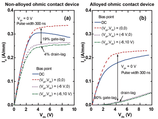
Figure 2: Pulsed current-voltage measurements in air at 0V gate potential for (a) non-alloyed and (b) alloyed devices.
Current collapse, and gate and drain lag, were assessed using pulsed measurements (300ns width, 0.5ms period). The gate lag was 90% for the alloyed HEMTs while the non-alloyed devices reduced this to 19% (Figure 2). The gate lag in the non-alloyed HEMTs could be due to local air breakdown or residue traps. The 4% drain lag of the non-alloyed HEMTs could not be compared with a value for the alloyed devices since the gate lag in the latter case was so severe.
The researchers comment: "The small current collapse in the non-alloyed devices correlates well with its low gate leakage: the low leakage prevents electrons being trapped within hundreds of microseconds when the device is held at the off state. On the other hand, the high leakage in the alloyed device facilitates electron trapping and the electron emission rates from the traps are too low to recover the current, thus a severe current collapse."


