A team of researchers at the USA's Massachusetts Institute of Technology (MIT) and the Masdar Institute of Science and Technology in Abu Dhabi, United Arab Emirates has developed a new solar photovoltaic 'step cell' that combines two different layers of absorbing material arranged in a stepwise fashion — with the lower layer jutting out beneath the upper layer, exposing both layers to incoming sunlight — in order to harvest a broader range of the sun's energy. Such layered (multi-junction) solar cells are typically expensive to manufacture, but the researchers also used a novel, low-cost manufacturing process.
The step-cell concept can reach theoretical efficiencies above 40% and estimated practical efficiencies of 35%, prompting the principal investigators — Masdar Institute's Ammar Nayfeh, associate professor of electrical engineering and computer science, and MIT's Eugene Fitzgerald, the Merton C. Flemings-SMA Professor of Materials Science and Engineering — to plan a startup company to commercialize the solar cell.
Fitzgerald, who has launched several startups (including AmberWave Systems Corp, Paradigm Research LLC, and 4Power LLC) thinks that the step cells might be ready for the PV market within the next year or two.
The team presented its initial proof-of-concept step cell in June at the 43rd IEEE Photovoltaic Specialists Conference in Portland, OR, USA. The researchers have also reported their findings at the 40th and 42nd annual conferences, and in the Journal of Applied Physics and IEEE Journal of Photovoltaics.
Beyond silicon
Traditional silicon crystalline solar cells are relatively cheap to manufacture but are not very efficient at converting sunlight into electricity. On average, solar panels made from silicon-based solar cells convert 15-20% of the sun's energy into usable electricity.
Silicon's low efficiency is partly due to its bandgap energy, which prevents it from efficiently converting higher-energy photons (e.g. blue, green, and yellow light) into electrical energy. Instead, only the lower-energy photons (e.g. longer-wavelength red light) are efficiently converted into electricity.
In contast, gallium arsenide and gallium phosphide can harness more of the sun's higher-energy photons. While these semiconductors have reached higher efficiencies than silicon, the highest-efficiency solar cells have been made by layering different materials on top of each other and fine-tuning them so that each can absorb a different part of the electromagnetic spectrum.
Layered solar cells can reach theoretical efficiencies above 50%, but their very high manufacturing costs have relegated their use to niche applications such as on satellites, where high costs are less important than low weight and high efficiency.
The Masdar Institute-MIT step cell, in contrast, can be manufactured at a fraction of the cost because a key component is fabricated on a substrate that can be reused. The device could thus help to boost commercial applications of high-efficiency, multi-junction solar cells at the industrial level, it is reckoned.
Steps to success
The step cell is made by layering a gallium arsenide phosphide (GaAsP)-based solar cell on a low-cost silicon solar cell. The silicon layer is exposed, appearing like a bottom step. This intentional step design allows the top GaAsP layer to absorb the high-energy photons (from blue, green, and yellow light), leaving the bottom silicon layer free to absorb lower-energy photons (from red light) not only transmitted through top layers but also from the entire visible light spectrum.
"We realized that when the top GaAsP layer completely covered the bottom silicon layer, the lower-energy photons were absorbed by the silicon germanium (SiGe) — the substrate on which the GaAsP is grown — and thus the solar cell had a much lower efficiency," says Sabina Abdul Hadi, a PhD student at Masdar Institute whose doctoral dissertation provided the foundational research for the step-cell. "By etching away the top layer and exposing some of the silicon layer, we were able to increase the efficiency considerably."
Working under Nayfeh's supervision, Abdul Hadi conducted simulations based on experimental results to determine the optimal levels and geometrical configuration of the GaAsP layer on silicon to yield the highest efficiencies. Her findings resulted in the initial proof-of-concept solar cell. Abdul Hadi will continue supporting the step cell's technological development as a post-doctoral researcher at Masdar Institute.
At MIT, the team developed the GaAsP by growing the semiconductor alloy on a substrate made of SiGe.
"GaAsP cannot be grown directly on silicon, because its crystal lattices differ considerably from silicon's, so the silicon crystals become degraded," notes Nayfeh. "That's why we grew the GaAsP on the SiGe — it provides a more stable base."
The problem with the SiGe under the GaAsP layer is that SiGe absorbs the lower-energy light waves before it reaches the bottom silicon layer, and SiGe does not convert these low-energy light waves into current. "To get around the optical problem posed by the SiGe, we developed the idea of the step cell, which allows us to leverage the different energy absorption bands of GaAsP and silicon," says Nayfeh.
The step cell concept led to an improved cell in which the SiGe template is removed and re-used, creating a solar cell in which GaAsP cell tiles are directly on top of a silicon cell. The step-cell allows for SiGe reuse, since the GaAsP cell tiles can be under-cut during the transfer process. "We grew the GaAsP on top of the SiGe, patterned it in the optimized geometric configuration, and bonded it to a silicon cell," says Fitzgerald. "Then we etched through the patterned channels and lifted off the SiGe alloys on silicon," he adds. "What remains then is a high-efficiency tandem solar cell and a SiGe template, ready to be reused."
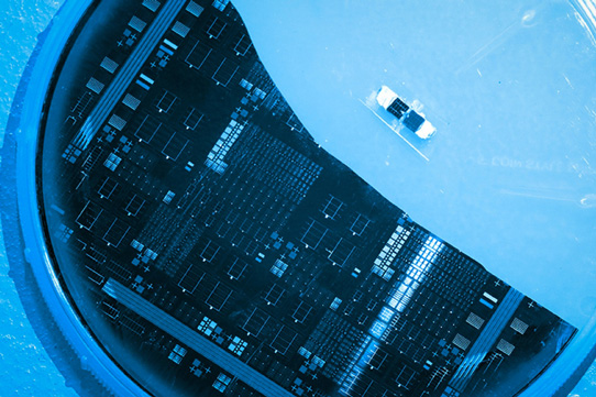
Picture: A silicon solar cell with SiGe filter using a step-cell design (large) and a GaAsP layer on silicon step-cell proof-of-concept solar cell (small). (Photo: Tahra Al Hammadi/Masdar Institute News.)
Because the tandem cell is bonded together, rather than created as a monolithic solar cell (where all layers are grown onto a single substrate), the SiGe can be removed and reused repeatedly, which significantly reduces the manufacturing costs.
"Adding that one layer of the GaAsP can really boost efficiency of the solar cell but, because of the unique ability to etch away the SiGe and reuse it, the cost is kept low because you can amortize that SiGe cost over the course of manufacturing many cells," Fitzgerald says.
Filling a market gap
Fitzgerald believes that the step cell fits well in the existing gap of the solar PV market, between the super-high-efficiency and low-efficiency industrial applications. Also, as volume increases in this market gap, the manufacturing costs should be driven down even further over time.
This project began as one of nine Masdar Institute-MIT Flagship Research Projects, which are high-potential projects involving faculty and students from both universities. The MIT and Masdar Institute Cooperative Program helped to launch the Masdar Institute in 2007. Research collaborations between the two institutes address global energy and sustainability issues, and seek to develop R&D capabilities in Abu Dhabi.
"This research project highlights the valuable role that research and international collaboration plays in developing a commercially relevant technology-based innovation," says Nayfeh.


