Researchers in Korea have been developing improved non-alloyed contacts for gallium arsenide (GaAs) complementary metal-oxide-semiconductor (CMOS) and high-electron-mobility transistors (HEMTs) [Seung-Hwan Kim et al, IEEE Electron Device Letters, 3 February 2016]. Four universities were involved: Korea University, Hanyang University, Sungkyunkwan University, and Inha University.
Source-drain contacts for GaAs devices are usually alloyed to reduce contact resistance. However, the high temperatures involved significantly increase surface roughness, and reliable devices then need large source-drain separations, which blocks attempts to scale to smaller dimensions. Also, surface roughness causes problems in gate fabrication.
To avoid contact metal alloying, the researchers have developed a zinc oxide (ZnO) interlayer to avoid metal-induced gap states (MIGS) and sulfur hexafluoride (SF6) plasma passivation to deal with interface traps.
The researchers used an n-GaAs wafer doped with silicon ~2x10¹⁸/cm3. The wafer was cleaned to remove organics and native oxides. The passivation of interface trap states consisted of either aqueous ammonium sulfide ((NH4)2S) solution treatment or plasma SF6.
Atomic layer deposition (ALD) at 250°C was used to apply zinc oxide from diethyl zinc precursor and water vapor reactant. The non-alloyed metal contacts consisted of 30nm titanium and 40nm gold, produced through electron-beam evaporation.
The ZnO interlayer metal-interlayer-semiconductor (MIS) structure was designed to block MIGS penetration, which induces Fermi pinning to the charge neutrality level (CNL), creating a Schottky barrier rather than ohmic contact. ZnO was chosen for its wide bandgap and small conduction band offset to GaAs, compared with alternatives such as aluminium oxide, silicon nitride or hafnium dioxide.
The SF6 passivation produced 36x higher current than non-passivated metal-semiconductor (MS) contact samples without ZnO interlayer (Figure 1). The performance was also much better than sulfur passivation from (NH4)2S solution. The optimum process time for the SF6 process was found to be 10 seconds.
Figure 1: (a) Current-voltage characteristics and (b) specific contact resistivity for titanium on SF6-treated n-GaAs as function of plasma process time. Inset in (a) shows schematic of electrical measurements of MS contact.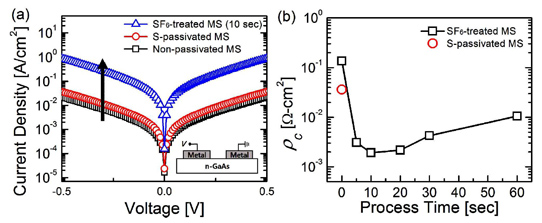
"These results signify that the proposed passivation method can effectively reduce the interface trap states on the GaAs surface," the researchers write.
X-ray photoelectron spectroscopy (XPS) suggested that 10 seconds was sufficient for the formation of Ga-S passivation bonds, whille avoiding a GaF3 electron tunneling barrier layer with 9.8eV bandgap and large conduction band offset.
Atomic force microscopy (AFM) showed that surface roughness increased negligibly from 0.357nm to 0.572nm root-mean-square.
The MIS samples with ZnO interlayer and SF6 passivation had currents 4x and 15x that of sulfur- and non-passivated MIS structures, respectively. The optimum thickness of ZnO was found to be 1.3nm. Above this, tunneling resistance becomes significant. The lowest MIS specific contact resistivity (ρc) was ~8x10⁻⁶Ω-cm2 for 1.3nm ZnO and 10-second SF6 passivation (Figure 2).
Figure 2: (a) Current-voltage characteristics and (b) specific contact resistivity for MS contact and MIS contacts. Insets in (a) show the band diagram of MIS contact (left) and schematic of electrical measurements of MIS contact (right).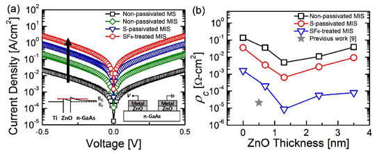
The researchers say that this is around a 10-4 reduction on the non-passivated titanium-GaAs MS contact. They add: "This ρc value is also lower than that of the Ge-passivated MIS contact in our previous work."
The MIS contact with SF6 also had almost the same electrical characteristics after annealing at 450°C for two hours.


