| Driven by market demand, the semiconductor industry progressed toward consensus on building-block standards for automating LED production on 6-in wafers at the Semicon West conference, explains PAULA DOE.
| |
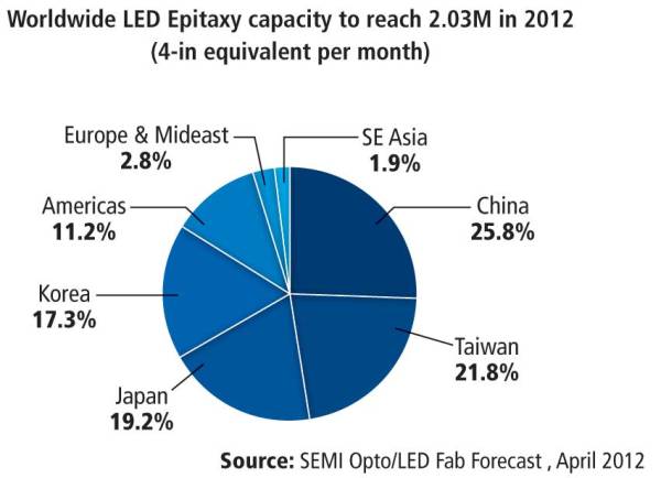
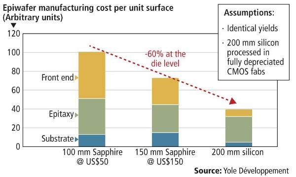
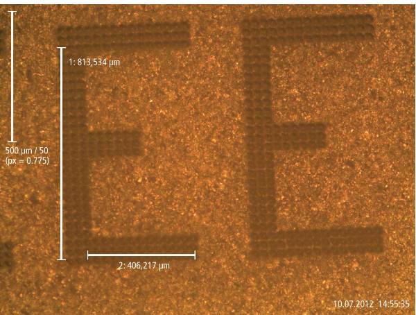
| With the fast-growing demand for HB-LEDs, the industry has added roughly 100 new fabs in the last five years, for a total of 169 LED fabs worldwide. That's pushed total industry epitaxy capacity to balloon by 5×, to some 2 million (4-in equivalent) wafers a month (Fig. 1). But the sector still has considerable headroom to improve yields and reduce costs to drive the growth of the solid-state lighting (SSL) market by moving to larger diameter wafers and automated production with tighter process controls. The major players are making good progress on the ground work to enable this transition, by collaborating to forge consensus on the basics of common wafer parameters, common interfaces for production equipment, and common communication software to communicate data from analysis tools. Fig. 1. LED 2012 fab capacity by region. Compelling economics Lower front-end processing costs for 6-in wafers mean about a 25% cost savings compared to 4-in wafers, per unit surface area, if yields are the same, estimated Eric Virey, senior LED analyst at Yole Développement, in discussions on HB-LED manufacturing solutions at the recent Semicon West event (Fig. 2). That assumes the larger wafer costs come down to about $150, 3× as much as the $50 4-in wafers. Though the larger wafers are still more costly per unit area, more die per process pass makes production more efficient, and the yields are better, so the product cost is less. "We see the advantage that the newer generation [6-in] equipment is much better and gets better yields than 3-in," said Iain Black, VP of manufacturing engineering at Philips Lumileds, and one of the co-chairs of the SEMI (Semiconductor Equipment and Materials International) HB-LED standards effort. Conversion to the larger diameter wafers will take a little longer than originally expected, as LED makers currently have excess capacity on their 2-in and 4-in lines, and fast falling 4-in wafer prices have made 4-in more competitive, said Virey. But prices of 6-in wafers are also falling quickly, and they could drop below $200 by the end of the year. Yole expects more than 25% of the total sapphire wafer surface area processed will be on 6-in wafers within the next two to three years, 50% a few years thereafter. Improving chip manufacturing process yields is the low hanging fruit for bringing down SSL costs to drive market growth, concurred Jed Dorscheimer, managing director of equity research for lighting and solar at Canaccord Genuity. He noted that process yields were typically 65%-70% at the market leaders, and only 10% at some newcomers, compared to >95% for the semiconductor industry. Small yield losses at each process step compound quickly into big yield hits. He figures good progress in improving yields over the next two years could realistically help enable a $7-$8 60W-equivalent LED bulb by about 2014, propelling the general lighting industry to surpass displays as the main driver of the LED market. One key enabler of these gains is basic standards for materials and equipment interoperability. "Standards are needed to mature the supply chain," said Black. "We've put considerable effort into our specs to upscale the capabilities of the supply chain. Others can reap the benefits of this work, but it's still a young industry and the vendors need to mature their processes. If we are able to establish decent standards, then everyone knows what to chase, and it will drive capability much more readily. If every spec is unique, we will get there much more slowly. For automation, it's good that we can innovate mostly around established semiconductor industry standards, but we need to get the differences squared away for common cassettes and handling of bowed wafers so we can need to do as little invention as possible." Silicon wafers? If 6-in sapphire gives such an improvement in yields and cost, what about the potential of larger silicon wafers? Eight-inch silicon could potentially give a 60% cost improvement at the die level – provided the yields were equal, Virey reported (Fig. 2). Though the wafers are significantly cheaper, the real advantage here too is not the substrate cost, which is only 5%-10% of the bill of materials, but the highly efficient and automated mature semiconductor infrastructure, especially if using a fully depreciated CMOS fab. The key problem to solve remains thermal mismatch, which causes more wafer bow and strain that impacts yields, which still remain significantly below sapphire, though somewhat lower yields could be acceptable with the lower costs. Most major companies have research programs, but the jury remains out on if silicon will be a widely viable replacement for sapphire. Fig. 2. Potential cost benefits of larger 6-in sapphire wafers and moving to 8-in silicon wafers. Hanmin Zhao, CTO of Lattice Power Corp, a China-based startup funded by some $120 million in largely US venture capital, reported his company is now selling commercial LED die from volume production runs of several hundred wafers a day on 2-in silicon wafers. The company uses stress reduction layers of AlN (aluminium nitride) and AlGaN (aluminium gallium nitride) to reduce bow to 20-30 µm to eliminate cracking, yielding 120 lm/W in production for a 45-mil chip. The company is working on scaling production to 6-in wafers in the lab, and looking for available production facilities to start production next summer.Wafers cassettes and capacity Automating HB-LED production naturally requires some basic agreement on the physical characteristics of the wafers so the equipment can be designed to handle them. Taking the coming transition to 6-in substrates as a clean-slate opportunity to optimize the process from the beginning, most of the major suppliers and device makers have joined in a collaborative effort to reach consensus on basic wafer parameters and interoperability standards, with meetings at Semicon West and other industry events. Now thanks to hard work by some 160 volunteers from across the industry, the first SEMI standards for 6-in sapphire wafer parameters and common wafer cassettes and software protocols for automation are moving through the consensus building process. The automation task force has agreed to keep the external dimensions of the cassette for handling 6-in sapphire wafers in the automated process flow the same as the standard 25-wafer cassettes used for semiconductor manufacturing, so it fits the storage racks and other infrastructure already available. Discussions at Semicon West considered the issues around how many of the thicker and more bowed sapphire wafers could most efficiently be carried by each cassette. Wider pockets within the cassette are needed, but tool makers need to settle on a common size and spacing of these slots to automate the handling and tracking of the wafers. "A standard cassette format will help drive interoperability between tools, and reduce capital costs and manufacturing costs," notes Jeff Felipe, Entegris' regional product specialist lead and SEMI automation task force co-chair. If the carriers take 12 wafers, spaced to correspond to every other slot of the 25-wafer cassettes, the automation and wafer process tools can handle and track the LED wafers with the existing semiconductor software. But the smaller capacity cassettes would mean that batch equipment, such as metal organic chemical vapor deposition (MOCVD), may need to install an additional load station for efficient throughput. Alternatively, the LED cassettes could take 16 wafers to maximize their capacity and avoid the need to install additional loading stations. That option would come at the cost of requiring extra handling steps to transfer the wafers back to 12-wafer cassettes for the rest of the process line, or requiring revision of the rest of the equipment software to handle the different format. The industry committee is currently soliciting input on this issue from LED makers worldwide before the end of October. Software and communication interfaces On the software side, the key initial issue is a common communication interface to make it simpler for LED makers and their equipment suppliers to get the data out of the tool to monitor production quality. "Higher automation needs well established data acquisition and monitoring to control production at the fab level," notes Karl-Heinz Buechel, Aixtron program manager for corporate control systems and the subgroup leader of the software working group in the SEMI automation task force. Fig. 3. Example of dot-matrix laser marking, which is being tested for survivability, courtesy of InnoLas Semiconductor. The task force analyzed the available options of the semiconductor industry interface called SECSII/GEM (SEMI equipment communications standard/generic equipment model), another SEMI standard called Interface A, and XML and concluded that a system based on SECSII/GEM could meet current and future requirements for LED manufacturing. Interface A may be considered for future needs for higher bandwidth for enhanced engineering data acquisition.The LED sector will, however, need to develop its own solution within SECSII/GEM to handle its unique need to track wafers on the graphite process trays within the batch tools by wafer, position and process. And it will need to decide whether to base its own SECSII/GEM applications dialect on the simpler 200-mm-wafer version commonly used on the legacy process tools, or whether it needs the more advanced capabilities of the 300-mm version. The task force is now polling LED makers to determine the most important functions users need, so equipment makers can all get that data out of the tool in a consistent way to feed into the device makers' data analysis system. "Making a custom communications system for each customer just increases the cost of the tool and the cost of integrating the data across the process," notes Buechel. "The secret sauce of the LED maker is analyzing the data, not in getting the data out of the machine and formatting it." Common wafer parameters The automation interface work can move forward because the 6-in wafer task force has largely reached consensus on the basic standard parameters for 6-in sapphire wafers, which should also help drive the quality and consistency of the wafer product. "With more industry standard specs we can then produce higher volumes of the same product with tighter control and lower cost, compared to making so many custom products," said David Reid, Chongqing Silian Optoelectronics COO, and a co-chair of the SEMI HB-LED standards committee. The wafer task force solicited input from players around the world to reach agreement on wafer features ranging from physical geometry like thickness and edge profile, to conventions of wafer marking and fiducials, to quality requirements like back side roughness, amount of warp and surface condition. "The legacy specs that were in use didn't really capture what's important to our customers today," noted Reid. "We needed a common way to talk about things, and to capture expectations as well as specifications." The standards will include both 1.0-mm and 1.3-mm thicknesses, and both notches and flats, as all are widely used, although with time the industry will likely move towards the thinner wafers and the smaller notches as fiducials. Collaborating companies also reported on their joint work to figure out solutions to some new issues posed by automation and process control systems, such as how to uniquely mark the sapphire wafers for tracking so that the identifying marks survive the processing. Current wafer IDs are not necessarily unique: some users want a mark on the front of the wafer for ease of reading, some want the mark on the back side for better survivability, and some want marks on both front and back just in case. The task force has devised a standard marking system with billions of unique options for each supplier, and Silian, InnoLas Semiconductor and Osram Opto Semiconductors are working together to test the survival of various deep laser marking systems through wafer processing. InnoLas marks test wafers from Silian with various dot-matrix and alpha-numeric figures with a UV laser (Fig. 3). Osram will then process the wafers and test the marks for readability. Results are expected by October. The dot matrix marking would be preferred if the dots can successfully be made deeply and distinctly enough to survive processing, as it takes up less wafer area and is easier to check. The group is now starting a new effort to determine which bulk and surface wafer defects have the most real impact on product yield, and to agree on common best practice methods to measure those parameters. Other SEMI work in Asia, driven by Epistar and TSMC in Taiwan, is focusing on environmental health and safety issues for HB-LED production, aiming at specifying best practices for installing and operating production equipment to a common worldwide standard. The group is working to complete and extend the existing semiconductor safety standards to more specifically apply to the LED manufacturing process, with its MOCVD tools and pyrophoric gases. "We're trying to change the world's lighting industry," notes Reid. "No one company can do it alone." |


