Mass production of GaN template wafers based on sapphire substrates could free LED manufacturers' MOCVD reactors for more LED production and lower component cost helping drive the deployment of SSL.
Hitachi Cable has become the second manufacturer in less than a year to announce plans to mass produce gallium nitride (GaN) template wafers, based on sapphire substrates, that reduce the processing steps that LED manufacturers must handle in their MOCVD (metal organic chemical vapor deposition) systems. Hitachi, like Silian and Soitec, plans to use the less-expensive and faster HVPE (hydride vapor phase epitaxy) process to build the templates upon which LED manufacturers will then build their unique LED structures using metal organic vapor phase epitaxy (MOVPE) in MOCVD reactors. The proposition aims to reduce manufacturing time and reduce LED cost, and that in turn could drive a quicker transition to solid-state lighting (SSL).
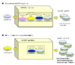
Hitachi points out that MOVPE efficiently yields the thin atomic-level active layers required in a blue LED that ultimately delivers phosphor-converted white LED. But MOVPE is extremely slow in growing the much thicker n-type GaN buffer layer that is sandwiched between the sapphire substrate and the active layers.

Typical GaN LED structure
HVPE is widely used in making many colors of indicator LEDs and is less expensive and faster than MOVPE. Fewer chemicals are required in HVPE, and the process does not require precursor gases that are very expensive. Moreover HVPE offers a faster epitaxial growth rate, and can yield the requisite buffer layer according to proponents.
Hitachi Cable had previously developed HVPE technology to grow GaN substrates for blue-violet lasers. The company has evolved that work to develop mass-production capability of GaN templates.

MOVPE process simplification
Presumably, LED manufacturers will still be able to leverage their unique LED structures in the MOVPE process performed on the templates. Indeed Hitachi said that it will also offer templates with patterned sapphire substrates (PSS) -- a widely used production technique aimed at optimizing light extraction.
Hitachi Cable says that an MOCVD reactor can produce one or two runs of white epiwafers per day. The company didn't say how many more runs could be made using templates, our earlier story linked above said that 60% of reactor capacity is freed up in some cases. Hitachi Cable said that 2-6-in templats are available and that it would offer 8-in templates in the future.
Template wafers are only one of many approaches being pursued to lower LED manufacturing cost. A transition to silicon substrates is another, and Azzurro in fact is developing silicon-based templates. Moreover, a simple move to larger sapphire substrates, sticking with the MOVPE process, could yield savings according to ARC Energy.
About the Author Maury Wright is the Editor of LEDs Magazine and Illumination in Focus.


