Researchers in Russia claim “the first demonstration of an injection quantum well microdisk laser fabricated of III-V materials monolithically grown on silicon (001) substrate” [N. V. Kryzhanovskaya et al, Optics Express, vol. 25, p16754, 2017]. Up to now, reports of microdisk lasers on silicon have used optical pumping rather than the electrical injection needed for optoelectronic applications.
Scientists and engineers are seeking to combine III-V light-generating technology with silicon photonics for many applications such as optical telecommunications. Monolithic direct growth of III-V materials on silicon is preferred over heterogeneous integration methods such as wafer bonding. Monolithic integration should reduce process complexity, cutting costs and increasing yields.
St Petersburg Academic University, Peter the Great St. Petersburg Polytechnic University, Ioffe Physical Technical Institute of the Russian Academy of Sciences (RAS), Institute for Physics of Microstuctures of RAS, and the Lobachevsky State University of Nizhny Novgorod, used molecular beam epitaxy (MBE) to produce templates that consisted of germanium (Ge) on exact (i.e. less than 0.5° offcut angle) (001) Si substrate.
An initial 275°C 50nm Ge layer, aimed at two-dimensional growth and island suppression, was followed by a 600°C 1μm Ge buffer. The low-temperature step allowed strain relaxation by misfit dislocation generation, while presenting a flat surface for further high-quality growth at high temperature. The template was then annealed with five cycles of 850°C/550°C for 2 minutes at each temperature.
Figure 1: Cross-sectional scanning electron microscope (a) and transmission electron microscope (b,c) images of the epitaxial structure.
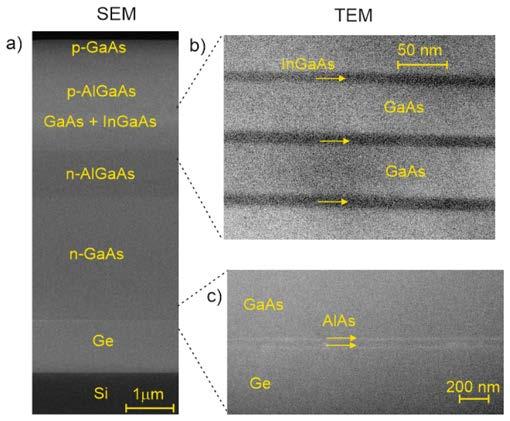
The template was cleaned before metal-organic chemical vapor deposition (MOCVD) of III-V layers (Figure 1): 10nm AlAs, 50nm GaAs, 10nm AlAs buffer; 2.5μm n-GaAs current spreader; 0.8μm n-GaAs waveguide; 1μm n-Al0.3Ga0.7As cladding; active region; 1μm p-Al0.3Ga0.7As cladding; and 0.8μm p-GaAs waveguide. The active region was three 10nm InGaAs quantum wells with average InAs content of 17%. The n-type silicon doping was achieved with silane. Carbon tetrafluoride was used for p-type carbon doping.
Microdisk resonators were formed using photolithography and inductively coupled plasma etch to a depth of 3μm. The p-contact metal consisted of silver-manganese/nickel-gold. The diameter of the metal contact was 4μm less than that of the microdisk. The common gold-germanium/nickel/gold n-contact was deposited on the region between the microdisks.
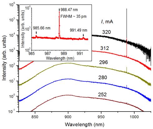
The pulsed-injection turn-on voltage of the devices was around 1.2V, in line with the expected optical transition energy. A 31μm-diameter device had a knee in the intensity of the 988.47nm-wavelength dominant mode at 0.31A injection current, suggesting a lasing threshold (Figure 2). The linewidth was 81pm at minimal current, which reduced to 35pm at threshold. The dominant mode was an order of magnitude greater than side modes at threshold, increasing up to 20dB side-mode suppression with increasing current injection. As the current increase continued, the dominant mode was quenched and side modes began lasing.
Figure 2: Electroluminescence spectra taken at different currents for 31μm-diameter microdisk laser. Spectra vertically shifted by 10dB for clarity. Inset: close-up spectrum near threshold (312mA).
Smaller 27μm- and 23μm-diameter microdisks had lasing thresholds at 160mA and 131mA, respectively. The 27μm device had the smallest threshold current density of 28kA/cm2. This is five times higher than for edge-emitting lasers of similar III-V structures, according to the researchers. The team blames non-radiative recombination at the microdisk sidewalls, suggesting also that this factor is to blame for the lack of lasing in devices with 21μm-diameter disks and smaller. Passivation could help to reduce surface recombination.


