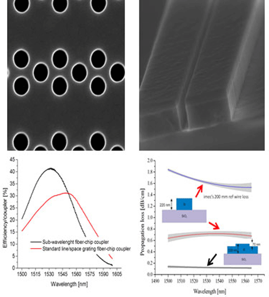
In conjunction with the SEMICON West 2012 event in San Francisco,CA,USA(10-12 July),nanoelectronics research center Imec of Leuven,Belgium has announced what it claims is the first realization of functional sub-100nm photonics components with optical lithography on 300mm silicon photonics wafer technology.Using 193nm immersion lithography,it has achieved the lowest propagation loss ever reported in silicon wire waveguides,and patterned simpler and more efficient fiber couplers.

Graphic:Left(top)Deeply etched sub-wavelength photonic crystal fiber-chip coupler and(bottom)its coupling efficiency in comparison to standard line/space grating based fiber-chip couplers;right(top)photonic wire direction couplers with 100nm coupling gap and(bottom)propagation loss of photonic wire.
Imec's industrial affiliation program on optical I/O explores the use of photonics solutions for realizing high-bandwidth I/O in high-performance computing systems.The program is developing Si photonics processes,devices and circuits using CMOS fabrication processes.Until now,many nanophotonics components have only been demonstrated using lab-scale techniques such as electron-beam lithography.Imec says that it has demonstrated functional Si nanophotonics devices on industry-compatible 300mm wafers using 193nm immersion lithography and 28nm CMOS processes.Imec says that its achievement is a key step in bringing silicon photonics technology into line with CMOS industry standards and hence industry adoption.
The optical waveguides on 300mm wafers have a very low propagation loss,well below 1dB/cm.Moreover,Imec patterned sub-wavelength features and demonstrated optical fiber-chip couplers using 193nm immersion lithography.By applying 193nm immersion lithography for patterning waveguides as well as fiber couplers,Imec eliminated one patterning step in the processing of photonics devices,resulting in a significant reduction in processing cost,it is claimed.By demonstrating low phase errors on 450nm arrayed waveguide gratings(AWGs),Imec says that its patterning platform using 45nm mask technology and 193nm immersion lithography has proved it can yield a very uniform waveguide width within a device.
"Our achievement with 193nm immersion lithography and 28nm CMOS processes on 300mm wafers is an important step in Si photonics development to demonstrate the manufacturability of highly integrated components,"reckons Philippe Absil,director of the optical I/O program at Imec."Possible applications are next-generation short-reach interconnects,which we expect to go into manufacturing by 2015,"he adds.
The results were obtained in cooperation with INTEC(Imec's associated lab at Ghent University)and Imec's key partners in its core CMOS programs(Globalfoundries,Intel,Micron,Panasonic,Samsung,TSMC,Elpida,SK Hynix,Fujitsu,Toshiba/Sandisk,and Sony).


