Researchers in China have designed and constructed a two-stage 2.5-5GHz low-noise amplifier(LNA)using enhancement-mode(normally-off)aluminium gallium arsenide(AlGaAs)pseudomorphic high-electron-mobility transistors(pHEMTs)[Peng Yangyang et al,J.Semicond.,vol33,p105001,2012].The researchers comment:"According to the author's knowledge,this is the lowest-power-consumption LNA fabricated in 0.5μm AlGaAs/GaAs pHEMT[technology]with comparable performance."
LNAs have many wireless applications such as radar(S-band 2-4GHz;C-band 4-8GHz),ultra-wideband data communications,and software-defined radios.
Gallium arsenide monolithic microwave integrated circuit(MMIC)technology competes against silicon technology and may soon have to seriously contend with gallium nitride(GaN)devices.Although silicon-based components can achieve cut-off frequencies up to 300GHz,GaAs technology is widely used in critical components for microwave and millimeter-wave application due to its greater reliability and high yield.GaN devices can achieve higher gain,but at higher cost and with higher power consumption.
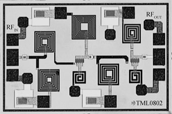
 Figure 1:Chip photograph of LNA.
Zhejiang–California Nanosystems Institute and Zhejiang University jointly developed the circuit that included on-chip capacitors and inductors,and measured 1.5mm x?1mm(Figure 1).The design aimed at flat gain over a frequency range and standard 50Ωimpedance matching for the input and output.A wideband matching network and a negative feedback were used to achieve the researchers'aims of wide operation bandwidth and low noise figure.
The average small-signal gain of the circuit was 17dB with flatness of 1.6dB over the frequency range 2.5-5GHz.The input and return losses over this band were less than 10dB.The bias conditions were achieved with 1.5V power supply(VDD),giving a gate bias of 0.7V and drawing a total current of 22mA(IDD).
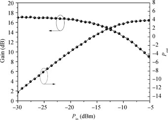
 Figure 2:Power performance of the LNA at 4GHz.
The noise figure was 2.4dB to 3dB for frequencies from 2.5GHz to 5GHz at a current bias of 33mA.From power performance measurements(Figure 2),the 1 dB compression point(P1dB,the power level that causes the gain to drop by 1 dB from its small-signal value)was found to be 2.3dBm with total power consumption of 33mW.Another measure of non-linearity/gain compression,the third-order intercept point(IIP3),was-2dBm.
The author Mike Cooke is a freelance technology journalist who has worked in the semiconductor and advanced technology sectors since 1997.