Researchers based in France and Germany have developed techniques for growing indium arsenide (InAs) channel structures on silicon [L. Desplanque et al, Appl. Phys. Lett., vol101, p142111, 2012]. Room-temperature mobility for the epitaxial material was an extremely high 27,800cm2/V-s.
The researchers were associated with Institute of Electronics, Microelectronics and Nanotechnology (IEMN) of France's CNRS and University of Lille, German company NAsPIII/V GmbH, Philipps-University Marburg, and Centre de Recherche sur les Ions, les Matériaux et la Photonique (CIMAP).
InAs channels are among the options for future high-electron-mobility devices for mass production. For such low-cost production, devices using such channels need to be incorporated into large-diameter silicon wafer processes.
In combination with aluminium antimonide (AlSb), which has a large conduction-band offset and small lattice mismatch with InAs, extremely high electron mobility has been achieved on indium phosphide (InP) and gallium arsenide (GaAs) substrates. However, up to now high-quality crystal material has been difficult to grow monolithically on silicon due to the lattice mismatch of 12% between the InAs and Si. Such a discrepancy tends to lead to anti-phase domains (APDs) and other structural problems that degrade electron transport performance.
The researchers began their work by optimizing the growth of AlSb/InAs layers on (001) gallium phosphide (GaP) substrates (Figure 1, structure A) using a Riber 32P molecular beam epitaxy (MBE) reactor. The purpose of this optimization was particularly to avoid APDs. Using these results, the researchers then performed MBE on 4cm x 4cm GaP/Si templates (Figure 1, structure B).
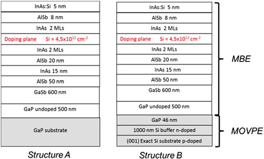
Figure 1. Schematics of AlSb/InAs heterostructures grown by MBE on GaP substrate (structure A) and grown by MOVPE and MBE on exactly oriented silicon substrate (structure B).
The templates were produced by metal-organic chemical vapor phase epitaxy (MOVPE) on 300mm (001) +/-0.5° p-doped Si wafers. The MOVPE reactor was an Aixtron Close Coupled Showerhead CRIUS system. The GaP growth surface was strained pseudomorphically to the structure of the Si substrate without any misfit or threading dislocations.
The resulting heterostructures were analyzed with atomic force microscopy (AFM), transmission electron micrography (TEM) and x-ray diffraction (XRD). Hall measurements were carried out on mesa bridge and van der Pauw structures with alloyed indium contacts, carefully annealed at 180°C for 2 minutes in the case of structure B to ensure ohmic contact while avoiding short-circuiting the InAs channel through the n-type doping plane.
The researchers used AFM surface morphology studies to explore the tradeoff between relaxation and rapid island coalescence of the gallium antimonide (GaSb) buffer layer by reducing both the temperature and the Sb flux during growth of the nucleation layer. After nucleation, the growth temperature and flux can be raised to improve the GaP template surface. The use of GaSb buffer gives tensile-strained InAs layers.
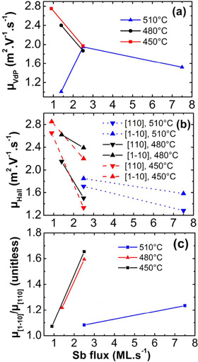 Figure 2. Transport measurements on heterostructures grown on GaP substrates with different temperatures and Sb fluxes during the first 50nm of GaSb buffer layer: (a) room-temperature van der Pauw electron mobility (μVdP), (b) Hall Bridge measurements (μHall) in different crystal directions, and (c) anisotropy of electron mobility deduced from (b).
The optimum condition for nucleation was found to be 450°C with Sb flux of 0.9ML/s (monolayers per second), giving heterostructures on GaP substrates with smooth surfaces of 0.8nm root-mean-square (RMS) roughness. These conditions also resulted in the best Hall properties (Figure 2) with the sheet carrier density at 1.5x10¹²/cm2, giving room-temperature (300K) van der Pauw electron mobility at 27,800cm2/V-s, and 77K mobility at 120,000cm2/V-s.
Having found the optimal growth conditions on GaP substrate, the recipe was transferred to GaP/Si templates. Again, AFM gave RMS roughness of 0.8nm. The van der Pauw Hall effect measurements on structure B with sheet carrier density 1.5x10¹²/cm2 gave room-temperature mobility at 27,800cm2/V-s and 77K mobility of 111,000cm2/V-s.
There is almost no anisotropy in the mobility, indicating the usefulness of the InAs structure for the realization of high-speed and low-power-consumption electronic devices, according to the researchers.


