LayTec AG of Berlin, Germany (which makes in-situ metrology systems for thin-film processes, focusing on compound semiconductor and photovoltaic applications) says that at last October’s International Workshop on Nitride Semiconductors (IWN 2012) in Sapporo, Japan, Jonas Hennig of Germany’s Otto-von-Guericke Universitat Magdeburg reported on high-performance gallium nitride (GaN) high-electron-mobility transistor (HEMT) structures on Si(001) with highly optimized interlayers to control stress and defect density. According to Hennig, in-situ growth monitoring using LayTec’s Epi-Curve TT helped greatly with strain engineering.
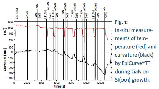
Figure 2 (below) demonstrates pronounced Fabry-Perot oscillations at 633nm (blue) and 950nm (red) in correlation with smooth development of curvature, which shows the high quality of the GaN. Furthermore, during the growth of interlayers, when the temperature is being brought down, an abrubt increase of curvature can be observed, as shown in Figure 1 (above).
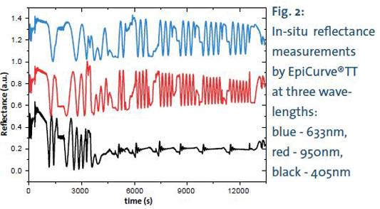
The three combined reflectance signals help to determine the growth rates and adjust the growth parameters. Additionally, the 405nm reflectance (Figure 2 - black) provides information on the structural interface quality.
The work at Otto-von-Guericke University and other institutions that use LayTec’s in-situ tools for silicon applications shows that the quality of GaN/Si can be significantly improved by advanced curvature monitoring combined with multiple wavelength reflectance, says LayTec.


