Suzhou Institute of Nano-tech and Nano-bionics (SINANO) in China has been using double-gated nitride semiconductor high-electron-mobility transistors (HEMTs) to understand the effects of field-plates in improving dynamic performance [Guohao Yu, IEEE Electron Device Letters, vol34, p217, 2013, published online 15 January].
Nitride HEMTs are being intensively developed for high-power electronics in high-frequency amplification and power switching applications. Often high performance in DC operation is lost when the HEMT is switched – for example, the on-current collapses when the gate signal is pulsed. It is thought that such effects are related to charge trapping that masks the effect of the gate on current flow. Field-plates on the source and gate electrodes have been used to manipulate the electric field in the device, mitigating such current-collapse phenomena.
SINANO proposed and fabricated the double-gate device “for the first time” in an effort to understand the action of such field-plates. With understanding, the researchers hope to further improve nitride HEMT performance and to bring these devices closer to wide commercial application.
The nitride semiconductor heterostructure (Figure 1) was grown on sapphire by metal-organic chemical vapor deposition (MOCVD). The gallium nitride (GaN) buffer was 2μm thick, separated from a 30nm Al0.3Ga0.7N barrier by 1nm of AlN. The structure resulted in a two-dimensional electron gas (2DEG) channel with sheet resistance of 400Ω/square, mobility 1080cm2/V-s and carrier density 1.44x10¹³/cm2.
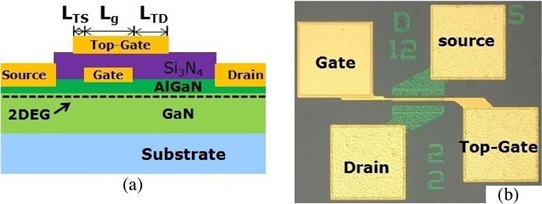
Figure 1: (a) Schematic cross-section of AlGaN/GaN DG-HEMT. (b) Optical image of DG-HEMT.
Mesa isolation of the transistors was achieved with a chlorine/boron trichloride plasma etch. The ohmic contacts consisted of titanium/aluminium/nickel/gold annealed at 850°C for 30 seconds in nitrogen. The gate electrode was nickel/gold. The top gate with the same composition was deposited on 165nm of silicon nitride (Si3N4). The electrode pads were accessed by etching through the SiN dielectric.
The device dimensions were: gate-source spacing 5μm, gate-drain 12μm, gate width 100μm, gate length 2μm, top-gate overhang towards source (LTS) 2μm, and top-gate overhang towards drain (LTD) 4μm.
The HEMT structure (top-gate floating) had a negative threshold (normally-on/depletion mode) at -3.4V, ~34mA 10V drain current at +1V gate potential, and +1V gate on-resistance of 115Ω.
The dynamic testing of the device was designed to mimic the behavior of source field-plate (SFP) and gate (GFP) field-plate by suitable biasing of the top gate. The SFP mode was achieved by grounding the top gate at 0V throughout the test cycle. The GFP mode consisted of biasing the top-gate in step with the ordinary gate at +1V for the on-state and -5V for the off-state.
The falling delay time (τfd) was measured as the time taken for the output voltage to fall to 10% of the peak-to-peak value (Figure 2). The dynamic on-resistance (Ron_D was also measured by the average from this 10% time up to the next switch-off point.
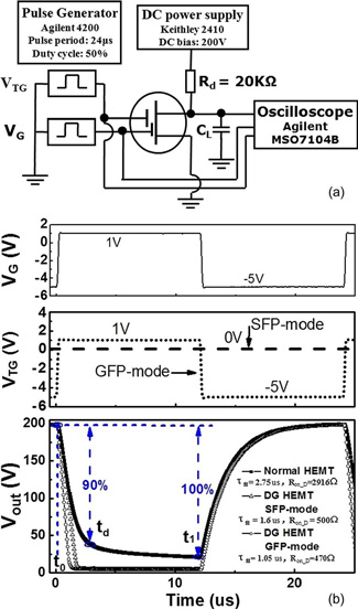
Figure 2: (a) Schematic of the dynamic testing system. (b) Input pulse signals and drain output voltage (Vo) waveforms of a DG-HEMT working at the SFP and GFP modes and in a normal HEMT.
The results show that without field-plates, the HEMT structure suffers from serious degradation due to switching: the falling delay time is 2.75μsecs and the dynamic on-resistance is 2916Ω. Both the SFP and GFP setups give distinct improvements, with the GFP-mode giving the best results of 1.05μs delay and 470Ω on-resistance.
The researchers explain: “In the AlGaN/GaN HEMT, the peak electric field usually locates under the drain-side gate edge; the higher the peak electric field is, the more charges are trapped in the regions adjacent to the gate electrode during the OFF-state. The FPs, i.e. both the SFP and the GFP, can effectively suppress the peak electric field by leveling the electric-field distribution underneath the gate electrodes; therefore, less charge is trapped. As a result, the dynamic performances can be much improved.”
While the above setup mimics the behavior of standard field-plates, the researchers also explored different biasing conditions of the double-gate. For example, with 5V gate and 0V top-gate off-state and +1V gate and 20V top-gate on-state, the delay was reduced to 0.78μs and the dynamic on-resistance was lowered to 430Ω. The improved behavior is attributed to partial compensation of the 2DEG carrier loss to charge trapping by the higher potential top-gate.
The researchers also looked at changing the negative top-gate potential during the off-state and having 0V top-gate during the on-state (Table 1). The most negative value tested had a similar delay to the previous case of 0.8μs. However, the on-resistance was reduced to 420Ω. The researchers suggest that the improved performance here could be due to suppression of electron injection/trapping from the gate edge into the AlGaN barrier in the off-state.
Top-gate voltage τfd Ron_D -5V 1.25μsecs 480Ω -10V 0.93μsecs 440Ω -15V 0.8μsecs 420Ω
Table 1: τfd and Ron_D versus off-state top-gate voltage.
The researchers conclude that the GFP improves dynamic performance more than the SFP does, which is explained by two factors: 2DEG compensation during the ON-state; and less negative charge trapping during the OFF-state.


