Reducing noise at high frequency in nitride-on-silicon transistors
France’s Institute of Electronic, Microelectronic and Nanotechnology (IEMN) has produced the first benchmark for low-noise gallium nitride on silicon transistors in the KA (26.5–40GHz) band [F. Medjdoub et al, IEEE Electron Device Letters, published online 26 July 2012]. “To the best of our knowledge, this low noise performance is the best reported so far for any GaN-based transistors at such high frequency of operation,” they say.
Possible applications of KA band millimeter-wave (mmW) technology include broadband radio links for cellular base-station networking, local multipoint distribution system (LMDS) data transmission, satellite communication and high-performance radar. Implementation of low-noise capability on low-cost silicon is expected to drive such developments. Previous reports of low noise for nitride semiconductor transistors at frequencies greater than 20GHz have been restricted to those produced on more expensive silicon carbide (SiC) or sapphire substrates.
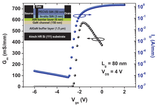
Figure 1. Transfer characteristic of a 0.08μm x50μm AlN/GaN/AlGaN DHFET on silicon substrate at VDS = 4V. Schematic cross section of device appears in inset.
The transistor’s aluminium gallium nitride (AlGaN) epitaxial double heterostructures (Figure 1 inset) were grown at EpiGaN in Belgium using metal-organic chemical vapor deposition (MOCVD) on highly resistive (111) silicon (4-inch diameter). The resulting material had an electron sheet concentration of 2.1x10¹³/cm2, mobility of 1300cm2/V-s, and resistivity of 230Ω/square, as revealed in room-temperature Hall measurements. The ohmic source-drain electrodes consisted of titanium/aluminium/nickel/gold annealed at 850°C for 30 seconds in nitrogen. The devices were isolated using nitrogen implants.
The Schottky gate structure consisted of 450nm of nickel/gold. The gate included a 0.2μm field-plate extension toward the drain to improve both breakdown voltage and gate resistance. The gate-source and gate-drain distances were 0.3μm and 1.2μm, respectively. The dual-gate width was 2x25μm (50μm total).
The maximum DC output current density of the device was 1.62A/mm at a gate potential of +2V (Figure 1). The extrinsic transconductance was 600mS/mm. The high value was attributed to high carrier density in the conducting two-dimensional electron gas (2DEG) and the thinness of the AlN barrier. The gate current leakage was less than 1μA/mm. The drain leakage was microamps/mm. The off-state breakdown (1mA/mm) was at 80V.
Pulsed testing was used to quantify drain-lag and current-collapse effects. The absence of current collapse was attributed to the in-situ SiN cap layer that helps to neutralize surface charge effects by avoiding surface contamination and native oxide formation as well as enhanced electron confinement due to the AlGaN back barrier.
Frequency performance (S-parameters) measurements were made over the range 1-50GHz. The extrinsic cut-off (fT) and maximum oscillation (fmax) frequencies were 95GHz and 105GHz, respectively, for a 100nm gate-length device. These values were increased, respectively, to 118GHz and 145GHz for an 80nm gate-length transistor. The optimum bias conditions were -1.8V gate bias, and 4V drain bias.
Figure 2. Associated gain and minimum-noise figure as a function of frequency biased at VGS = 1.8V and VDS = 4V at room temperature of 100nm and 80nm AlN/GaN/AlGaN-on-Si DHFET.
The researchers comment: “The frequency performance mainly results from the high transconductance and ultrashort gate lengths but are still limited by the RF loss at the buffer/Si interface that has been measured with standard transmission lines as high as 1.5dB/mm.”
The researchers finally measured noise figures (NFs) and associated gain (GA) for the 100nm and 80nm gate-length devices. At 40GHz, the NFmin for the 80nm device was 1dB (1.68dB for the 100nm transistor), while GA remained above 6dB. The optimum bias conditions were used. Record values of NFmin at 0.97dB and GA of more than 7.5dB were obtained at the slightly lower frequency of 36GHz.
The researchers believe that, since the optimal NF systematically corresponds to maximal GA, unique monolithic integrated circuit designs may be realized using the transistor.
The high performance is attributed to the high fT and fmax, along with good resistance performance of the source-drain access and gate, low gate leakage, and low DC to RF dispersion.
The researchers conclude: “The reported KA band GaN-on-Si minimum noise performances are comparable to best-class GaAs devices with the significant advantage of having a ten times higher breakdown voltage. Consequently, such devices are a promising candidate for cost-effective ultra-robust low-noise amplifier applications in next-generation millimeter wave communication networks.”
Tags: GaN/Si HEMTs MOCVD IEMN

 Water Ripple Effect Gobo Projector Light")


