Researchers at Purdue and Harvard universities have developed gallium arsenide (GaAs) enhancement-mode (E-mode) surface/n-channel metal-oxide-semiconductor field-effect transistors (NMOSFETs) with a maximum drain current of 336mA/mm, which is claimed to be a record high for such devices [L. Dong et al, IEEE Electron Device Letters 34 (4) p487; published online 7 March 2013, DOI: 10.1109/LED.2013.2244058].
The performance was enabled by atomic layer epitaxy (ALE) of the gate dielectric and annealing to reduce interface trap densities. Such traps kill performance by collecting charge that shields the gate, reducing its electrostatic effectiveness.
The NMOSFETs (Figure 1) were produced from semi-insulating GaAs 2-inch wafers. The crystal orientation used was (111)A, which avoids As-As bonds on the GaAs surface. Such bonds can lead to pinning of the Fermi level, killing device performance.
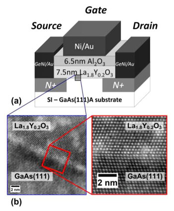
Figure 1: (a) Cross section of a GaAs(111)A surface channel E-mode NMOSFET. (b) High-resolution TEM image and enlarged view of single-crystalline GaAs – single-crystalline La1.8Y0.2O3 interface after 860°C RTA annealing. Epitaxial La1.8Y0.2O3 forms flat and sharp interface on GaAs(111)A substrate.
Dielectric deposition followed a number of surface preparation steps designed to degrease the wafers, remove native oxide layers and passivate the surface. The ALE dielectric stack consisted of 7.5nm lanthanum yttrium oxide (La1.8Y0.2O3) and 6.5nm aluminium oxide (Al2O3). The Al2O3 was used to protect the lower dielectric layer from reacting with water molecules from the air and from the following process steps. The equivalent oxide thickness of the structure was around 4.5nm.
Metal-organic precursors were used: lanthanum tris(N,N’-diisopropylformamidinate), yttrium tris(N,N’-diisopropyl-acetamidinate), and trimethyl-aluminium. The oxygen source was water. Atomic layer epitaxy consisted of pulsing the precursors. The chamber was purged with nitrogen after each water vapor pulse. Water molecules and/or hydroxyl groups trapped in the deposited material degrades crystallinity and dielectric permittivity.
Further fabrication consisted of implanting the source-drain regions with silicon to create n+-type semiconductor regions. The implant was followed by rapid thermal annealing (RTA) at 860°C for 15 seconds in nitrogen for dopant activation. The metallization of the source-drain regions consisted of gold/germanium/nickel/gold stacks defined by lift-off photolithography. Ohmic contact was created through more RTA at 400°C for 30 seconds in nitrogen. Further lift-off photolithography created a nickel/gold gate electrode.
The resulting devices were 100μm wide with various gate lengths (0.5-40μm). MOS capacitors (formed in a similar way on n- and p-type substrates, but without source-drain regions) were also produced for capacitance-voltage analysis of dielectric/semiconductor interface traps.
An NMOSFET with 0.5μm-long gate had a maximum drain current of 336mA/mm (Figure 2), described as a “significant improvement of the on-state current compared with the previously reported GaAs (111)A NMOSFETs with amorphous Al2O3 as the gate dielectric”. The peak current was achieved at 5V gate and 2V drain biases.
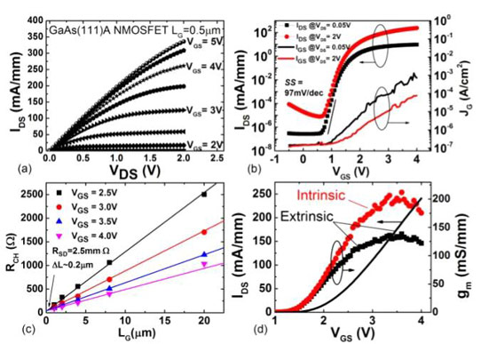
Figure 2: (a) Current-voltage (I-V) characteristic of 0.5μm-gate-length GaAs NMOSFET with ALE La1.8Y0.2O3 oxide. (b) Transfer characteristics and gate leakage current density of same GaAs NMOSFET as (a). (c) Measured channel resistance versus different mask gate-length as a function of gate bias. Source-drain resistance (RSD) of 2.5\Ohm-mm and ~0.2μm for the difference of the designed and effective gate-length (ΔL) are determined from fitting lines. (d) Extrinsic and intrinsic transconductance (gm) and extrinsic drain current versus gate bias of the same GaAs NMOSFET in (a).
The researchers believe that the high quality of their novel La1.8Y0.2O3 epitaxial interface passivates dangling bonds on the GaAs surface, reducing the number of interface traps.
The channel mobility peaked at 310cm2/V-s at an inversion charge density of 2x10¹²/cm2. The researchers believe that the drive current and mobility could be further enhanced by using buried channel structures or high-mobility channel material such as InGaAs.
The on/off current ratio was more than 107 with a drain bias of 2V (on = 2.3V gate, off = 0.5V gate). “This high ION/IOFF ratio is a promising feature for GaAs as compared to InGaAs, since the latter usually suffers from high S/D leakage current as a result of its relatively narrower bandgap,” the researchers comment.
The subthreshold swing was 97mV/dec across the range of gate lengths produced, again suggesting low interface trap densities in the mid-gap region.
The gate leakage increased from ~10-7A/cm2 to ~10-3A/cm2 as the gate bias increased from 0V to 4V. Despite this, the leakage remains at least five orders of magnitude smaller than the drain current up to 4V.
The maximum intrinsic transconductance for the 0.5μm-long gate NMOSFET was ~210mS/mm. The extrinsic value (i.e. not correcting for source-drain resistance) was ~138mS/mm. The researchers believe that the device transconductance could be further improved by reducing the dielectric thicknesses.
Capacitance measurements confirmed the importance of annealing for reducing interface trap densities from around 3x10¹²/cm2-eV to 5.5-7x10¹¹/cm2-eV. The significant reduction is seen as key to realizing high performance in the surface channel GaAs transistors.
The work at Purdue University was supported by the Air Force Office for Scientific Research (AFOSR). The work at Harvard University was performed at the Center for Nanoscale Systems (CNS), a member of the US National Nanotechnology Infrastructure Network (NNIN).
 Window for CO2 Laser Application")


