BluGlass has utilized its low temperature RPCVD process to develop p-type GaN, an essential material that make up the top layers of a nitride LED.
Preliminary testing has been carried out on the sample using a 0.5mm diameter size p-type indium contact. The light output was measured with a UV-detector positioned under the wafer calibrated at the wavelength of the light emission.
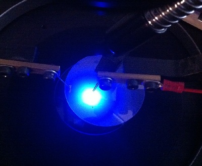
At 20mA and 4.7V, the light output was 270µW (light emission at 458nm with a full width half maximum of 19nm)
At 50mA and 5.5V, the light output was 1.23mW (light emission at 456nm with a full width half maximum of 18nm) - the current was applied continuously for over an hour without the loss of function of the device.
BluGlass recently outlined at the company's AGM, that it was looking to demonstrate p-GaN and identified a number of steps in order to demonstrate improved LED efficiency with a low temperature process.


