In 2014, the Nobel Prize in physics was awarded for the discovery of the gallium-nitride-based blue-light LED and its use for new, efficient LED-based white lamps. The development efforts in this field, however, do not stop there. The active layers in this type of diode take up less than 1μm. This means that most of the material in planar LEDs now on the market, which are hundreds of micrometers thick, is not used. This provides a motivation to continue research on efficient LEDs with nanoscale dimensions.1
In the last few years, it has been shown that an efficient LED can be made as a 3D nanostructure, in which the active parts take up less than 1μm. This makes more efficient use of the materials involved and, at the same time, excludes structural defects that limit the LED performance from the active device volume. Nanometer-sized LED structures can take many different shapes, such as thin elongated wires, pyramids, cubes, or platelets. To grow each of these small objects, different sections—including contact layers and an active region where the light is produced—are used. Basic material properties, however, put constraints on what can be grown, which affects the choice of shape for the nano-LED. For visible-light LEDs, the III nitrides—gallium nitride (GaN), aluminum nitride, indium nitride, and their alloys—are very suitable since they offer bandgaps in the visible range of photon energies.
We have recently summarized the current status of the development of nanowire-based LEDs.1 These devices are mainly shaped like nanorods with hexagonal cross sections, where the different layers are grown in a concentric manner around a core section (see Figure 1). The active region that produces the light consists of indium gallium nitride (InGaN) quantum wells (QWs) on m-plane facets, where 'm' refers to a specific crystallography orientation. Such QWs do not suffer from any polarization fields since the m-plane is non-polar. All other layers in the structure—the core, underlayer, QW barrier layers, p-layer and p-contact layer—are grown from GaN. A disadvantage with this design is that emission wavelengths longer than green are difficult to produce because of limitations with incorporating indium in the m-plane. Furthermore, there is a large lattice misfit strain built into the active QW region for high concentrations of indium corresponding to long wavelengths. This eventually causes defects and a reduced radiative efficiency for the LED.
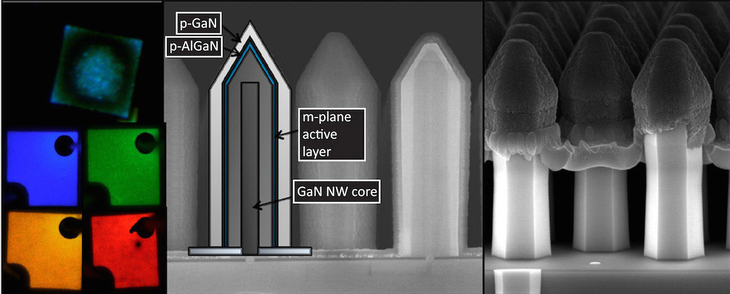
Figure 1. Top left: Electroluminescence from the first blue nanowire LED fabricated by Glo AB in April 2007. Bottom left: Blue, green, yellow, and red examples from current state-of-the-art nanowire LEDs, grown by Glo-USA Inc. in 2013. Center: Side-view of a scanning electron microscope (SEM) image, showing nanowire LEDs monolithically grown on a wafer of gallium nitride on silicon. The edge of the top contact layer is visible, and both the contacted and non-contacted LEDs can be seen. Right: SEM image illustrating the air-bridge process. Images provided courtesy of QuNano AB and Glo AB.1 p-GaN: p-Type gallium nitride. p-AlGaN: p-Type aluminum gallium nitride.
In our latest work,2 we aim to solve these problems. The main concept driving our research is the need to create a ternary InGaN alloy in the form of a fully relaxed and dislocation-free c-oriented micro-substrate, where 'c' refers to another crystallography orientation. Our basic idea is to use the c-plane for the growth of the main LED structure, which improves the indium incorporation, with the use of a pre-fabricated indium-containing c-facet. This provides an opportunity to extend the possible emission wavelengths towards the red (see Figure 2). To handle the polarization fields existing in the c-plane structures, all layers in the structure should be made of InGaN, thereby reducing the strain. Importantly, this also also relaxes the otherwise stringent limitation on the QW width (because of the piezoelectric field in the QWs), which is typical for planar c-plane structures.
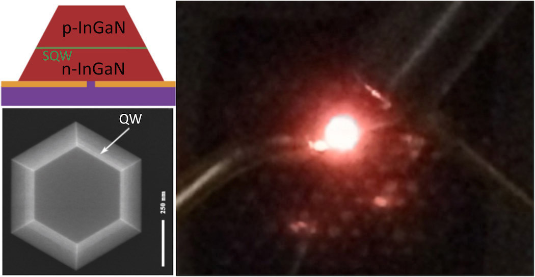
Figure 2. Top left: Schematic side-view cross section of a red-emitting LED. Bottom left: Top-view SEM image of a vertically grown pn-junction. The scale bar indicates 250nm. Right: Electrically driven red-emitting LED for the structure shown to the left. n/p-InGaN: n-Type/p-Type indium gallium nitride. QW: Quantum well. SQW: Single QW.
In our work, we demonstrate how a unique sequence of growth and processing steps—initiated by a nanowire structure—enables the formation of c-oriented platelets of fully relaxed, still dislocation-free, InGaN micro-substrates. On top of these substrates, it is now possible to grow dislocation-free, more indium-rich InGaN QWs that are designed to emit throughout the green to red spectral range. We have not yet established the typical efficiency of these LEDs, but we estimate it to be a few percent at present. This is considerably better than for typical planar red LEDs, even though these efficiencies were reached without any real optimization efforts.
In summary, we have shown that InGaN-based nano-LED structures show promise for solving the problems associated with long-wavelength nitride LEDs. There is a demand for LEDs covering all visible wavelengths using the GaN-InGaN material system. The first applications of our device, which does not require very high output power from the LEDs, may be for display technology. In fact, we can fabricate InGaN nano-LEDs that emit at blue and green wavelengths in one processing step on the same wafer. This provides additional opportunities and flexibility for display design. In the future we aim to create a flat substrate on to which we can form an active QW with an even higher indium-concentration, corresponding to emission of longer wavelengths (e.g. green, yellow, and red).
Lars Samuelson Lund University and Glo AB NanoLund, Sweden
Lars Samuelson is a professor and a member of the Royal Swedish Academy of Sciences (physics). In 2014 he was awarded the Fred Kavli Distinguished Lectureship in Nanoscience. He is the primary founder and chief scientific officer of the companies QuNano AB, Glo AB, Sol Voltaics AB, and Hexagem AB.
Bo Monemar Lund University NanoLund, Sweden
Bo Monemar was a professor and head of the Semiconductor Materials Division at Linköping University from 1983 to 2009. He is still active in research at this university, and works part-time at Lund University and the University of Tokyo. His main research field is III-nitride materials. He has published about 1200 papers.
B. Jonas Ohlsson Lund University and QuNano AB NanoLund, Sweden
Jonas Ohlsson is an adjunct professor in semiconductor physics and epitaxy. He is involved in several nanowire startups, including QuNano AB, where he is director of research, Glo AB, where he was director of epitaxy from 2008 until 2012, and Sol Voltaics AB, where he is director of intellectual property and innovation. He is a co-founder of QuNano AB, Glo AB, and Hexagem AB.
Nathan F. Gardner Glo-USA Inc. Sunnyvale, CA


