Researchers based in the USA have used a double-heterostructuring based on order-disorder properties of aluminium indium phosphide (AlInP) to produce 'amber-green' light-emitting diodes (LEDs) [Theresa M. Christian et al, J. Appl. Phys., vol114, p074505, 2013]. The research involved collaboration of the US National Renewable Energy Laboratory, University of Colorado Boulder, and Massachusetts Institute of Technology.
Copper-platinum B-type ordering in AlInP consists of spontaneous segregation into alternating aluminium- and indium-rich (111) planes. One effect of the ordering is expected to be a reduced energy bandgap. A similar order-disorder structure is used in high-brightness aluminium gallium indium phosphide (AlGa)InP LEDs.
Production of LEDs with yellow (590-560nm) or green (560-490nm) emission is presently difficult commercially. The long- and short-wavelength ends of the visible spectrum are covered using phosphide and nitride semiconductor materials, respectively. The amber-green range constitutes a gap for the production of efficient LEDs.
Although white light LEDs presently use ultraviolet or blue LEDs with phosphors to create a spread of longer wavelengths in approximation to white, the color rendering is poor. A preferable solution, if it can be made economic, would be to combine light from four LEDs with different wavelength properties. A suggested combination of wavelengths is 459nm (blue), 535nm (green), 573nm (yellow/'amber'), and 614nm (orange). The blue and orange targets are well covered by existing technology.
The nitride semiconductor approach to longer wavelengths involves problems such as enhanced efficiency droop and difficulties in growing high-quality indium gallium nitride (InGaN) with high indium content.
From the non-nitride III-V semiconductors, the material with widest bandgap is AlInP. However, this option has not been researched extensively due to a lack of a convenient substrate and uncertainties about the material system's characteristics, such as the region of aluminium concentration for which the energy bandgap is direct.
The epitaxial structures were produced on gallium arsenide (GaAs) in a Thomas Swan/Aixtron low-pressure metal-organic chemical vapor deposition (LP-MOCVD) system with a close-coupled showerhead. Growth began with a 250nm homoepitaxial layer of GaAs before applying compressively graded InGaAs buffer with a lattice mismatch rate of 0.5%/micron. The 'virtual substrate' structure was capped with a constant-composition 0.7μm InGaAs buffer layer.
The LED layers consisted of a double heterostructure of AlInP n- and p-type cladding around an undoped active region (Figure 1). The cladding layers were grown at 725°C and the active region at 650°C. The lower-temperature growth of the active region was designed to promote ordering. The n- and p-type regions were achieved using silicon and zinc doping, respectively.
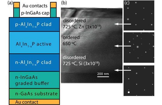
Figure 1: (a) Schematic of AlInP double-heterostructure LED device on graded InGaAs virtual substrate. (b) Transmission electron micrograph (TEM) of typical order-disorder heterostructure LED (device 1) with Al0.59In0.41P. Growth temperature and doping properties of active and cladding layers are indicated. (c) Transmission electron diffraction showing that both variants of CuPt-B type ordering occur in the active layer, but ordering is suppressed in cladding.
An InGaAs cap on the p-cladding was used to promote ohmic contact with the gold electrodes. The epitaxial structure was annealed at 425°C for a minute after the growth process. The gold on the p-side was in a grid form that was used as a mask for etch removal of the underlying InGaAs cap.
Three sample types were produced (Table 1) with different AlInP compositions. Also, in one case a (111)B substrate was used to suppress atomic ordering of the AlInP alloy. The other devices were grown on (100) substrates miscut 6° in the (-1-11) direction ('Miscut 6A'). Material grown on such miscut substrates tends to demonstrate improved material qualities such as better compositional homogeneity and surface smoothness.
Table 1: Selected properties of the AlInP devices.
Substrate Al fraction Active region EL peak (300K) Device 1 Miscut 6A 0.39 400nm 566 nm Device 2 Miscut 6A 0.36 300nm 600 nm Device 2B (111)B 0.36 300nm 586 nm
Preliminary photoluminescence studies on AlInP layers suggested that miscutting by 4° rather than 6° could lead to even greater ordering and hence narrower bandgaps. These studies also suggested that an optimal temperature for growing ordered material was around 680°C. The optimal bandgap shift achieved for Miscut 6A substrates was 180meV. Doping reduces the ordering effect.
The researchers comment: "Based on the reported results for bulk epilayer AlxIn1–xP films, we anticipate that bandgap differences between cladding and active layers in excess of 150meV can be achieved by optimizing our control of material ordering." However, the devices produced were estimated to have bandgap shifts of only 20-60meV, indicating room for improvement in the future.
A reference device with a GaInP active region and AlGaInP cladding was also produced on Miscut 6A substrates. The device used as reference was the brightest among several produced using conditions similar to those used for the AlInP devices. Commercial Ga0.51In0.49P LEDs can achieve external quantum efficiencies of more than 55%.
Pulsed current measurements were used to avoid self-heating affecting light output measurements. The current-voltage curves indicate that series resistance and other parasitic losses could be reduced to improve performance.
The light outputs of the 566nm (amber-green) and 600nm (orange ~ 590-635nm)-emitting devices at 1A/cm2 injection current density were, respectively, 23% and 39% that of the ~650nm (red ~ 700-635nm) standard GaInP reference device (Figure 2).
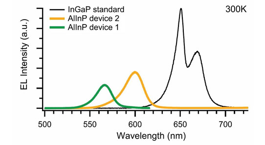
Figure 2: Comparison of room-temperature electroluminescence spectra for devices with mesa area 0.1cm2 at 100mA drive current (density 1A/cm2) for both AlxIn1–xP LEDs compared with reference Ga0.51In0.49P LED. Device 1 peaks at 566nm with full-width at half maximum (FWHM) of 20nm; light output is 23% as bright as GaInP standard. Device 2 peaks at 600nm with FWHM of 25nm; light output is 39% as bright as standard.
The researchers comment: "The performance of the AlxIn1–xP devices relative to a similar-quality unoptimized Ga0.51In0.49P device strongly indicate that an AlxIn1–xP material system holds promise for effective light emission in the amber-green wavelength range."
The disordered device 2B was compared with the ordered active region device 2. The researchers recognized the likely poorer quality of device 2B since it was grown using a process optimized for device 2. The light outputs were therefore normalized separately at 1A/cm2 to remove the material quality effect.
Beyond 1A/cm2, the light output from device 2 was relatively greater than for device 2B. At 40A/cm2, the boost from using an order-disorder heterostructure was a factor of three improvement in light output of device 2 over device 2B.
The degraded performance at higher current is consistent with the poor carrier confinement without the order-disorder heterostructure, according to the researchers.


