Oracle Networking Group in the USA believes that it has made the first demonstration of an integrated surface-normal coupled laser array on a silicon-on-insulator photonics platform [Shiyun Lin et al, Optics Express, vol24, p21455, 2016].
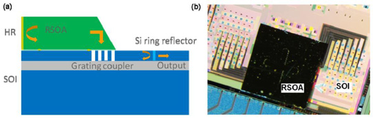
Figure 1: (a) Side-view schematic of surface-normal coupled hybrid laser, (b) microscope image of integrated 2x6 hybrid external-cavity laser array.
Passively aligned (i.e. laser off), high-accuracy flip-chip bonding was used to combine a III-V reflective semiconductor optical amplifier (RSOA) array with integrated total internal reflection mirrors onto CMOS silicon-on-insulator (SOI) containing silicon photonic circuits (Figure 1). The completed assembly formed a tunable hybrid external-cavity laser array.
The aim of the work is to fill the gap in silicon photonics for high-efficiency laser sources, giving a complete platform for next-generation optical interconnects that need large bandwidth, high density and high power efficiency.
The 2mmx2mm RSOA chip contained multiple quantum wells on indium phosphide (InP) with 600μm-long ridge waveguides in a 2x6 array. The pitch of the array was 1mm along the waveguide and 250μm perpendicular to this direction.
Chemically assisted ion-beam etch was used to create an angled mirror-facet. The light from the total-internal reflection mirror was angled to match the grating couplers (GCs) in the silicon photonics circuit. A further mirror on the back-facet of the RSOA was coated with material to give more than 95% reflectivity. The top surface of the chip was coated with anti-reflective material to reduce back reflection.
The photonic circuit was fabricated using a silicon-on-insulator substrate with 300nm silicon on 0.8μm buried oxide. A 130nm CMOS process was used to create a 2x6 array of ring reflector circuits that matched the RSOA chip (Figure 2). Silicon resistor micro-heaters were incorporated into the rings to provide laser wavelength tuning. Grating couplers were used to couple light into and out of the circuit. The light was output into a fiber array.
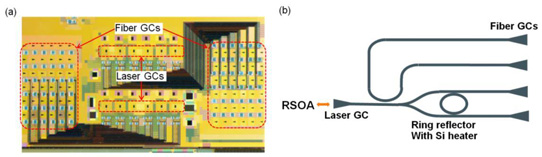
Figure 2: (a) Microscope image of CMOS SOI chip with 2x6 ring reflector circuit array, (b) schematic diagram of ring reflector design.
CMOS aluminium metalization provided bonding pads for the RSOA and metal traces to large probing pads. Under-bump metalization consisted of titanium-gold. Gold-tin (AuSn) bumps were sputtered on the CMOS pads.
The one-step passive bonding process had a peak temperature of 320°C. The RSOA and SOI chips were bonded using a high-accuracy flip-chip bonder with an alignment tolerance of ±0.5μm. The alignment was achieved in a one-step passive process with matching patterns near the coupling region. The demonstration used chip-to-chip bonding, but the researchers believe that the technique could be expanded to a wafer-scale pick-and-place set up. Indeed the automated bonding machine is designed for wafer-scale operation.
The maximum waveguide-coupled wall-plug efficiency (wcWPE) was 2%. The maximum optical power was greater than 3mW. The researchers described the efficiency as "relatively low" due to a large coupling loss between the RSOA and SOI chips. The researchers attribute this to a ~3dB coupling loss from the mode size mismatch between the III-V and the GC. The mode-field diameter of the RSOA was 1.3μm in the vertical direction and 2.0μm in the horizontal direction. The GCs had a diameter of 4μm in both directions. Also, there is a 14μm gap between III-V waveguide and GC that increases the coupling loss to 7dB. Increasing the III-V mode-field diameter to 3μmx3μm would reduce the coupling loss by ~3dB.
With the laser drive current at 80mA, the tunability range by heating was 1544-1556nm. The device stopped lasing outside this window. Reducing the output power ratio increased the range from 12nm to 19nm. The cross-coupling ratio was designed to be 50% for the top row of lasers in the RSOA and 25% in the bottom row. The tuning efficiency of both rows was 0.2nm/mW. The researchers believe this can be improved by localized substrate removal.
The team comments: "In order to improve the wcWPE, a smaller gap between III-V waveguide and silicon GC is desirable, and can be achieved by bringing the top metal closer to the InP layer and removing the unnecessary metal/dielectric layer stacks on the SOI chip. Together with a larger mode size, we believe a coupling loss of less than 3dB is achievable."
The researchers attempted to work towards improved wcWPE by fabricating a 1x6 array SOI chip with only a single metal layer rather than the full metal/dielectric stacking to reduce the gap between the component devices. A 2x6 RSOA was bonded onto the new SOI chip. The coupling ratio of the directional couplers was 50%. Platinum heaters were used for tuning. These factors reduced the gap to 10μm. The researchers estimated that this improved the optical coupling by 2dB. "The gap can be further reduced by optimizing the contact design on the RSOA chip and reducing the thickness of the AuSn bumps," the team writes.
Unfortunately, two of the channels of the new assembly were damaged in post-processing, leaving a 1x4 array of working lasers. The output power was ~10mW at 120mA drive current. The wcWPE was calculated at 5%. The team believes that a high-efficiency laser array could be achieved by further reducing the coupling loss by using a mode size converter on the RSOA chip to give a larger mode size.


