MEI Wet Processing Systems and Services LLC (a subsidiary of MEI LLC) of Albany, OR, USA has revealed performance data on its new Cu & TiW Critical Etch System for compound semiconductor manufacturing.
MEI says that its Critical Etch batch wet processing systems achieve comparable etch uniformity, providing superior results compared with single-wafer spray tools for Cu and TiW etch. Also, its critical etch solution enables consistent etching even within dense patterned areas. The immersion etch uniformity enables process engineers to minimize over etch times, the firm claims, enabling the use of lower-cost immersion technology to produce high-end products. The critical etch system also saves manufacturing floor space by reducing the wet process footprint requirement by at least 60% over comparable-throughput single-wafer spray tools, it is reckoned.
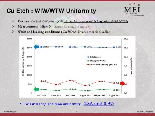
Picture: Performance data for MEI’s Cu & TiW Critical Etch System.
“MEI's Critical Etch solution for Au, Ag, Cu and TiW will allow semiconductor manufacturers to lower costs, reclaim valuable cleanroom space and increase yield while producing high-quality results," claims Dan Cappello, president & CEO of MEI LLC. “Our immersion system etch uniformity far surpasses many alternative solutions,” he adds. “Side by side ‘split lot’ comparison data demonstrates superior performance with <2% etch uniformity, compared to >15% for other immersion and spray tool designs.”
MEI says that it has leveraged its immersion experience so that, unlike conventional metal etch systems, its Critical Etch System is a low-cost, small-footprint, high-performance package. Systems can be configured for single or combination metal etch steps over a wide variety of needs. Whereas conventional etch solutions rely on dry tool or complex deplating processes that are very expensive to operate, MEI’s immersion solution enables a new generation of mobile devices to be produced in a cost-effective manner, the firm claims. MEI’s batch immersion systems are field proven on 1-5 micron features which were consistently etched with exceptional uniformity and high throughput.
The firm’s Critical Etch solution targets semiconductor and MEMS processing applications where metal pattern etches are required to create sophisticated mobile communication devices.


