Massachusetts Institute of Technology (MIT) has demonstrated gallium nitride (GaN) vertical Schottky and p-n diodes on silicon Si substrates “for the first time” [Yuhao Zhang et al, IEEE Electron Device Letters, published online 10 April 2014].
GaN is being developed for power electronics applications in both vertical and lateral structures. Although the lateral structure has been studied widely, it faces reliability and integration issues. Vertical structures have been realized more recently, but on high-cost small-diameter substrates such as free-standing GaN, silicon carbide (SiC) or sapphire. Potential advantages of vertical electronic structures include smaller chip sizes, better electric field profile with the peak away from the surface, and superior thermal characteristics.
The challenge for growth of GaN structures on silicon is to reduce dislocation densities resulting from the larger lattice mismatch compared with the alternative substrates.
The epitaxial structures for the MIT diodes (Figure 1) were grown on 3-inch (111) silicon substrates by metal-organic chemical vapor deposition (MOCVD). The estimated dislocation density in the GaN layers was ~109/cm3.
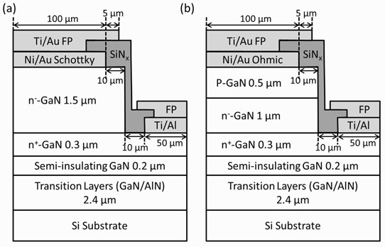
Figure 1: Schematic cross sections of GaN-on-Si vertical (a) Schottky and (b) p-n diodes with passivation and field plate structures.
The fabrication consisted of etch for mesa isolation and to access the cathode region (n-contact), deposition of titanium/aluminium in a ring n-contact, and then the deposition of 200μm-diameter nickel/gold circular anode contacts. The p-n diode included a p-GaN layer. For the Schottky barrier diode (SBD), the researchers deposited the anode metals directly on the top lightly doped (n-) n-GaN layer. The anode metals for the p-n diode were annealed at 550°C for 10 minutes in a nitrogen/oxygen environment to achieve an ohmic contact. The field plates (FP) consisted of silicon nitride passivation and titanium/gold metal bilayer.
The researchers developed two technologies to reduce leakage currents. First, a deep inductively coupled plasma reactive-ion etch for GaN, using chlorine/boron trichloride/argon plasma and a metal hard mask. The researchers write: “Under high ion bombardment energies, the use of metal hard mask could eliminate the erosion of mask edge usually observed when using traditional oxide hard mask, and therefore leads to a smoother vertical sidewall and a reduction in sidewall parasitic leakage current.”
The second technology was the silicon nitride passivation applied using a sputtering process with an optimized pre-clean. The passivation managed “to effectively reduce the dielectric/GaN interface leakage widely reported for traditional passivation using plasma-enhanced chemical vapor deposition (PECVD) systems.”
The p-n diode has higher ideality factor and on-voltage compared with the SBD due to the wide bandgap of GaN and higher resistance of the p-GaN layer, respectively (Table 1).
Table 1: Performance at 1A/cm2 forward current density.
Diode Ideality (n) On-resistance (Ron) On-voltage (Von) SBD 1.5 6mΩ-cm2 0.5V p-n 2.0 10mΩ-cm2 3.5V
The Schottky diode suffered destructive breakdown (BV) under reverse bias at 90V without field plate and at 205V with field plate. The researchers comment: “This demonstrates that the FP structure is effective in spreading the electric field at electrode edges, reducing the reverse leakage current and improving the reverse BV.”
The p-n diode has a soft breakdown (i.e. reversible) at 300V. At -200V reverse bias the leakage is 10-2A/cm2, a factor of three orders of magnitude better than that of SBD at the same bias. The p-n diode performance is also comparable to “state-of-the-art leakage reported for lateral AlGaN/GaN diodes on Si and SiC substrates”.
The researchers estimate a peak field of ~3MV/cm in the p-n diode under -300V reverse bias, “the highest in all reported GaN-on-Si devices,” according to the researchers. However, they point out that this is lower than the 3.4-3.7MV/cm reported for GaN-on-GaN structures, and the theoretically predicted critical field of 3.5-3.8MV/cm for GaN.
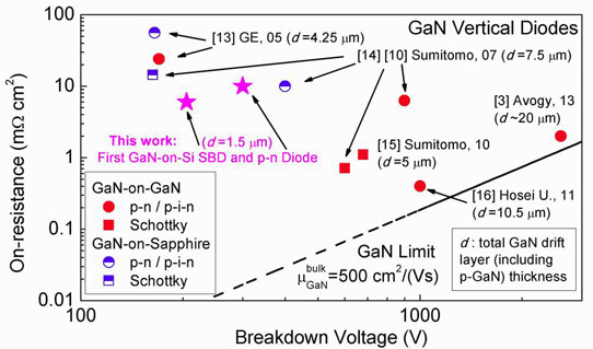
Figure 2: Specific on-resistance versus BV of MIT’s GaN-on-Si vertical diodes and GaN-on-sapphire and GaN-on-GaN vertical in previous reports. BV of GaN-on-Si vertical p-n diode is soft.
The researchers see their devices as providing a potential low-cost alternative to GaN-on-sapphire diodes (Figure 2), commenting that “considering the relatively thin drift layer (1.5μm) in our GaN-on-Si diodes compared to that typical in the GaN-on-sapphire (4-10μm) and GaN-on-GaN (5-20μm) diodes, our 200-300V BV results show great potential for low-cost GaN-on-Si vertical devices to outperform GaN-on-sapphire and GaN-on-GaN vertical devices with further improvement in GaN-on-Si growth technologies that enable a thicker and better-quality GaN drift layer on Si substrates.”


