Researchers at University of Notre Dame (UND) in the USA have claimed record high breakdown voltage for aluminium gallium nitride (AlGaN/GaN) lateral Schottky barrier diodes (SBDs) on silicon [Mingda Zhu et al, IEEE Electron Device Letters, published online 16 February 2015]. Two researchers from IQE LLC in the USA were also involved in the work.
The team achieved a breakdown voltage (BV) of 1.93kV (Figure 1). The researchers comment that "this BV value is the highest among the reported GaN-on-silicon diodes" and that the devices are comparable in performance with "state-of-the-art GaN diodes on SiC, sapphire and bulk GaN substrates". While devices grown on these latter substrates benefit from lower dislocation density in the nitride semiconductor material, the cost of silicon is much lower. Manufacturers, of course, want low cost combined with high enough quality for reliable power electronics applications.
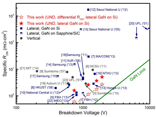
Figure 1: Benchmark plot of BV versus RON,SP. Reference values are re-calculated based on reported data using UND's definition of RON,SP to take into account diode turn-on effect (100mA/mm on-current). Differential RON of diodes also extracted (hollow stars) and modeled (dash line). Green line shows FOM limit of bulk GaN.
The University of Notre Dame SBD used epitaxial material grown on 6-inch (111) silicon by metal-organic chemical vapor deposition (MOCVD). The 100nm n+-GaN cathode ohmic contacts (Figure 2) were re-grown using molecular beam epitaxy (MBE). The cathode metal was unalloyed titanium/gold.
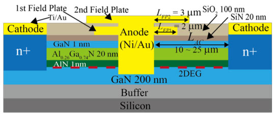
Figure 2: Schematic cross section of the recessed anode Schottky barrier diode with double field plates.
The recessed anode with two field plates was built in stages. First the silicon nitride (SiN) dielectric was deposited before the recess etch which drilled 50nm into the AlGaN/GaN layers. The nickel/gold (Ni/Au) for the recessed anode and first field plate was then deposited.
Finally, relative thick silicon dioxide (SiO2) and nickel/gold were used to form the second field plate. The SiO2 layer was chosen to be thick to support a large anode-cathode voltage drop. The anode-cathode distance (LAC) was varied between 10μm and 25μm.
The turn-on voltage of the device was around 0.67V. The reverse bias BV of 1.93kV (1mA/mm cut-off) was achieved with an LAC of 25μm. The devices had a specific on-resistance (RON,SP) of 5.12mΩ-cm2 at 100mA/mm forward current. The researchers also quote a power figure of merit (FOM = BV2/RON,SP) of 727MW/cm2. Corresponding values for a 20μm-LAC device were 1.6kV, 3.7mΩ-cm2, and 691MW/cm2. The researchers comment that the FOM values are comparable to other state-of-the-art devices.
The estimated switching time of the devices was ~350ps, despite the significantly increased capacitance of the double field-plate structure. The researchers estimate that the presence of the second field plate increased the BV by between 5% and 25%, dependent on LAC.
The researchers believe that there is room to improve the BV further by bringing the effective critical field closer to the value for bulk GaN with better engineering of the surface fields.


