Shigeya Kimura, Hisashi Yoshida, Toshihide Ito, Aoi Okada, Kenjiro Uesugi and Shinya Nunoue
Metal organic chemical vapor deposition is used to grow aluminum gallium nitride interlayers within indium gallium nitride/gallium nitride multi-quantum well structures on silicon substrates. 30 March 2016, SPIE Newsroom. DOI: 10.1117/2.1201603.006402
High-efficiency gallium-nitride-based LEDs have become widely popular as these devices have found several applications, e.g., as white LEDs in general lighting.1 Many of these LEDs are grown on aluminum oxide (Al2O3), silicon carbide (SiC), or gallium nitride (GaN) substrates.2 In addition, GaN-based LEDs grown on silicon (Si) substrates have attracted much attention because of their low fabrication cost. These GaN-based LEDs, however, tend to include high densities of dislocations and cracks because of the large mismatch of lattice constants and thermal expansion coefficients between the GaN-base layers and the Si wafers.3

Many groups have attempted to tackle this issue and have reported improvements in the manufacture of GaN-based LEDs.4, 5 For example, gas flow conditions and precise control of temperature in a reactor have been optimized.5 In addition, we have previously developed LEDs with low threading dislocation densities (TDDs), i.e., of less than 2 × 108cm2 on Si (111 crystallographic plane) substrates.6, 7 Those TDD values were almost the same as those of LEDs grown on Al2O3 (0001) substrates. We achieved this reduction of TDDs by using multiple modulations of dislocations during the formation of GaN islands on a silicon nitride (SiN) interlayer, and from the growth of the SiN cap layers on the GaN island surfaces. In the past, we have also confirmed that the external quantum efficiency (EQE) and the hot/cold factors (HCFs) of LEDs grown on Si (111) substrates increase with decreasing edge-type dislocations in the low-current-density region.8 We also showed that the EQE of a sample with a low TDD is almost as high as that of an LED grown on an Al2O3 (0001) substrate at room temperature.8
On the basis of our previous studies, in this work we have tried to further increase the efficiency of LEDs by using a functional multi-quantum well (MQW) structure on Si (111) substrates.9 Although many different types of MQW structures have already been suggested in this field,10, 11 we have paid particular attention to the structure to realize both a specific function and high crystallinity. We consider an indium gallium nitride (InGaN)/thin aluminum gallium nitride (AlyGa1−yN)/GaN MQW structure (where 0 ≤ y ≤ 1) to be one of the best candidates.
Schematic diagrams of the MQW layer structures investigated in our study are shown in Figure 1.9 Our reference MQW layer structure—see Figure 1(a)—consists of 3.5nm-thick In0.15Ga0.85N well layers and 5nm-thick GaN barrier layers. In contrast, the structure in Figure 1(b) has 1nm-thick AlyGa1−yN interlayers that replace part of the GaN barrier layers. These interlayers are in contact with the n-type (i.e., n-doped) side of the InGaN well layers, but we do not include any thin AlGaN interlayers on the p-type (p-doped) side of the InGaN well layers. According to the results of our band diagram simulation, a high density of hole carriers is expected to be induced in the thin AlGaN/InGaN heterostructures via spontaneous and piezoelectric polarization (caused by compressive stress in the thin AlGaN interlayers). These results also indicate that the internal quantum efficiency of those MQWs with thin AlGaN interlayers is enhanced compared with the MQWs that do not include the interlayers. This is because the radiative recombination rate is proportional to the multiplication of the distribution functions of the electron and hole densities.12
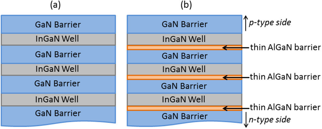
Figure 1. Schematic diagrams of the multi-quantum well structures investigated in this study. (a) A reference structure that consists of indium gallium nitride (InGaN) well layers and gallium nitride (GaN) barrier layers. (b) A structure with thin aluminum gallium nitride interlayers that partly replace the GaN barrier layers.
To grow our blue LED structures, we conducted metal organic chemical vapor deposition on 4-inch Si (111) substrates. After we had grown an AlN buffer layer on a chemically cleaned Si substrate, we grew an AlGaN buffer layer to prevent crack generation. In addition, a 2.5μm-thick u-GaN (i.e., undoped) layer with SiN interlayers was grown on the AlGaN layer. We have previously provided a detailed description of the AlGaN buffer layer structure and the properties of the i-GaN layer.6, 7 In the next step of our process, an n-GaN (i.e., n-type) layer, MQW active layers, and p-type layers were grown sequentially. Our target layer structures for the MQWs were those shown in Figure 1. We then used transmission electron microscopy, as well as energy dispersive x-ray spectroscopy and 3D atom probe analyses to confirm that the 1nm-thick AlyGa1−yN interlayers (where y was 0.3 or less) were continuously formed. Finally, we fabricated the thin-film LEDs by removing the Si (111) substrates from the grown layers. We also bonded Si support substrates on top of the p-type layers so that we could perform electroluminescence (EL) measurements.
The EQE of our LEDs—both with and without the thin Al0.15Ga0.85N interlayers—is shown as a function of current density, at room temperature, in Figure 2. The size of the measured LED chips was 0.5 × 0.5mm2. Our results show that the EQE of the LEDs with interlayers is enhanced compared with the sample that did not have interlayers in the low-current-density region. We obtained the peak EQE (82% at 4A/cm2) and HCF (94%) values by using the functional thin-AlGaN interlayers within the MQWs. The corresponding EL dominant wavelength was 444nm.
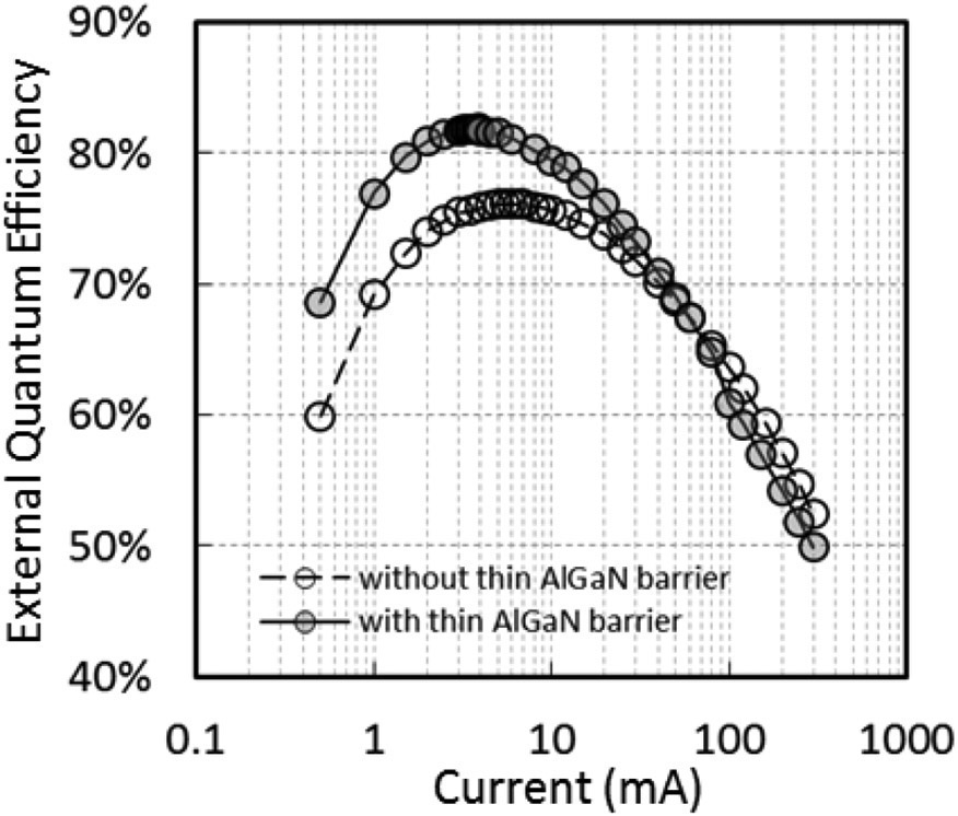
Figure 2. The external quantum efficiency of the LEDs, with and without the thin AlGaN interlayers, as a function of current density at room temperature. The LED chips were 0.5 ×0.5mm2 in size.
In summary, we have demonstrated high-efficiency blue LEDs that include thin AlGaN interlayers within InGaN/GaN MQW structures. In our technique, we place the functional MQWs on GaN underlayers that have low threading dislocation and on Si (111) substrates. The maximum EQE we obtain for such devices is very high compared with the value of blue LEDs grown on Si substrates. We are now investigating in detail the structural, optical, and electrical properties of our novel MQWs to enable their more efficient use.
Shigeya Kimura, Hisashi Yoshida, Toshihide Ito, Aoi Okada, Kenjiro Uesugi, Shinya Nunoue Toshiba Corporation Kawasaki, Japan
Shigeya Kimura is a research scientist in the Research and Development Center. He obtained his PhD in 2008 from Osaka University, Japan.


