Researchers in China and Turkey have been using varying-thickness gallium nitride (GaN) barriers between indium gallium nitride (InGaN) multiple quantum wells (MQWs) to improve hole distributions and thus to reduce efficiency droop effects in blue light-emitting diodes (LEDs) [Z. G. Ju, et al, Appl. Phys. Lett., vol102, p243504, 2013]. The idea for such a structure has been proposed before on the basis of simulations at Taiwan's National Changhua University of Education.
The new work at Nanyang Technological University, South University of Science and Technology of China, and Bilkent University, includes the growth and characterization of actual LEDs. The researchers conclude that the proposed graded-thickness quantum barrier (GTQB) structure only outperforms equal-thickness quantum barriers (ETQBs) at high current beyond 22A/cm2.
The epitaxial material was prepared on c-plane sapphire using metal-organic chemical vapor deposition (MOCVD). The substrate was patterned with cones of 2.4μm diameter and 1.5μm height at 3μm pitch. Growth began with 30nm of low-temperature GaN buffer and a 150nm GaN interlayer. A further 5μm of GaN and 3μm of silicon-doped n-type GaN were grown at high temperature.
The active MQW light-emitting region consisted of five 3nm InGaN wells grown at 750°C. The wells were separated by GaN barriers grown at 800°C. Material with equal-thickness 12nm barriers was used to represent conventional structures. Material with graded-thickness quantum barriers consisted of layers of 12nm, 7.2nm, 6.6nm, and 6.0nm thickness, which become gradually thinner towards the p-GaN contact.
The nitride semiconductor layers were completed with 30nm of Al0.2Ga0.8N as electron-blocking layers and 200nm p-GaN contact layers.
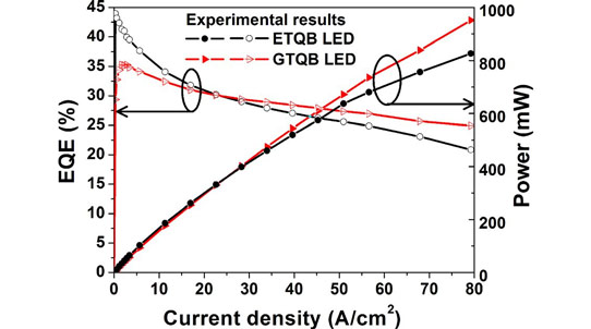
Figure 1. Experimentally measured EQE and light output power with increasing current density for ETQB and GTQB LEDs.
Electroluminescence was excited using indium contacts (Figure 1). The GTQB devices showed higher external quantum efficiency (EQE) and light output power above ~22A/cm2. The poorer performance below this current injection is attributed to the "weaker quantum confinement of the electrons within the QWs of the GTQB LED due to the thinner QB thickness."
At 70A/cm2, the light output power was 870mW, which is 13% higher than the comparison ETQB device (770mW). The droops from the maximum EQE were 28.4% for the GTQB LEDs and 48.3% for the ETQB devices. The researchers attribute improved optical power and EQE at high current density to better hole transport in the GTQB LED. As is often the case, improved droop performance comes at the cost of degraded peak EQE.
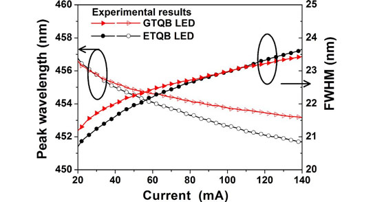
Figure 2. Experimentally measured peak wavelength and full-width at half maximum (FWHM) as a function of current for ETQB and GTQB LEDs.
Spectral measurements show blue-shifts and broadening of the linewidth at increased current for both devices (Figure 2). However, the shift and line broadening are smaller for the GTQB LEDs.
The blue-shift effect is often attributed to screening of the quantum-confined Stark effect (QCSE) caused by the electric fields resulting from strong piezoelectric (strain-dependent) polarization fields in the nitride semiconductors. With the thinner barriers in the GTQB material, one expects smaller strain fields in the MQW structure, reducing the QCSE.
The linewidth broadening is commonly associated with band-filling effects, which can be reduced by distributing the holes more evenly across the MQW region.
The researchers used numerical simulations of the LED structures under bias to help in interpreting the experimental results. In particular, the model can be used to explore electron-hole densities and recombination rates in the structure.
The thinner barriers near the p-GaN end were found to encourage a more uniform distribution of holes through the structure. Often, MQWs emit predominantly near the p-GaN end due to scarcity of holes reaching the deeper wells. Hole uniformity improved with the increase in injection current, according to the model.
In terms of the electron-hole recombination rate that determines light output, this was greatest near the p-GaN end in both ETQB and GTQB devices at low current (10A/cm2). At high current (70A/cm2), recombination increases in the deeper wells more significantly in the GTQB LED, compared with the ETQB structure.


