AlGaN/GaN and InAlN/GaN structures combine high electron mobility and high critical electric field strength and are excellent platforms for the production of next-generation RF and power electronics devices such as high-electron-mobility transistors (HEMTs), notes in-situ metrology system maker LayTec AG of Berlin, Germany. Their theoretical nearly three-orders-of-magnitude lower specific on-resistance compared with silicon-based devices could enable an at least 10-fold reduction in power losses, device size and cost, the firm adds.
Typically, the best performance is achieved on semi-insulating silicon carbide (SiC) substrates. However, the metal-organic chemical vapor deposition (MOCVD) growth of the AlGaN and AlInGaN structures on large SiC-4H wafers needs complex growth recipes for strain management and tight statistical process control (SPC) to obtain high process yields. For this technology, LayTec has therefore expanded its high-temperature nk database and implemented additional real-time analysis routines to feed SPC systems with highly accurate in-situ data.
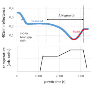
Picture: AlN buffer growth on SiC-4H in a three-step high-temperature process. The 405nm reflectance data is highly accurate due to auto-calibration to the true SiC-4H substrate temperature (blue – measured; red - fitted reflectance). The fit gives dAlN=73.2±0.5nm. (Data provided by confidential customer.)
In the example pictured, the initial AlN layer is grown on SiC-4H is performed at very high wafer temperature (measured by Pyro 400 with ±0.5K accuracy) in a sophisticated three-temperature process. This ensures signifiant defect reduction for the subsequent HEMT growth, says LayTec. Despite the varying wafer temperature in this AlN buffer growth process, the latest real-time analysis function of EpiNet library allows the firm's tools to reach ±0.5nm accuracy in real-time AlN fim thickness measurement. This has been achieved by tightly correlating the absolute SiC-4H wafer temperature with high accuracy SiC-4H and AlN nk optical data and implementing new analysis algorithms that separate reflectance changes caused by temperature ramping from the AlN growth effects, says LayTec.