University of California, Santa Barbara (UCSB) has used photo-electro-chemical etch (PEC) to create 405nm-wavelength vertical-cavity surface-emitting lasers (VCSELs) based on indium gallium nitride (InGaN) multiple quantum wells (MQWs) [C. O. Holder et al, Appl. Phys. Lett., vol105, p031111, 2014]
According to the researchers, VCSELs are attractive from a number of perspectives such as “circular output beam, single longitudinal mode operation, low output beam divergence, reduced threshold current, reduced device footprint, high modulation frequency, and characteristic vertical emission normal to the substrate, enabling the fabrication of high density 2D arrays.”
However, short-wavelength VCSEL devices based on nitride semiconductors such as InGaN are difficult to make. In particular, deposition of dielectric distributed Bragg reflectors (DBRs) on the n-side of the device requires the removal of the substrate. Methods to remove the substrate generally result in an undesired rough surface. UCSB has used PEC to create a smooth surface after substrate removal.
The epitaxial structure (Figure 1) was grown on m-plane free-standing GaN from Mitsubishi Chemical using atmospheric-pressure metal-organic chemical vapor deposition (AP-MOCVD). The substrate was misoriented 1° in the [000-1] direction to avoid the formation of pyramidal hillocks, as happens with on-axis growth.
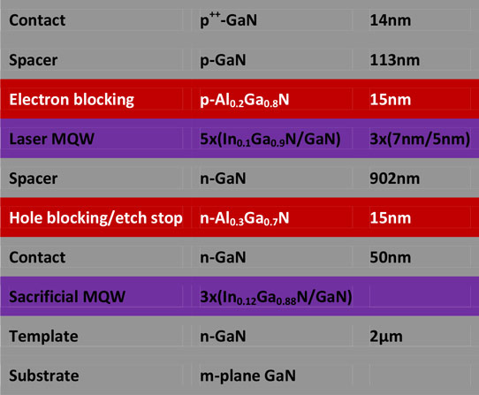
Figure 1: Epitaxial structure for m-plane VCSELs. Cavity length was designed at around 7.5 wavelengths.
The use of m-plane growth direction, rather than the more usual c-plane, was designed to avoid the problems of electric fields resulting from the spontaneous and piezoelectric (strain-dependent) polarization of nitride semiconductor alloys. Also, m-plane lasers have shown linear gain versus current characteristics, low transparency carrier and current densities, and high anisotropic gain.
The epitaxial material was formed into VCSELs that were flip-chip bonded onto a sapphire submount (Figure 2). The p-side DBR consisted of 13-period silicon dioxide/tantalum pentoxide (SiO2/Ta2O5) dielectric pairs.
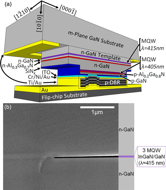
Figure 2: (a) Schematic cross-section of VCSEL following flip-chip bonding, but before native substrate removal. (b) SEM image of bandgap-selective PEC undercut etching for substrate removal.
The 415nm MQW part of the epitaxial structure was used as the active region for a PEC undercut etch that removed the substrate. The illumination above the 415nm bandgap was provided by a continuous wave (CW) 405nm laser at 200mW (65W/cm2).
The generated holes created the conditions for selective etch through oxidation of the gallium atoms in the sacrificial MQW layer. The electrolyte was potassium hydroxide solution. The photo-generated electrons were removed through a reduction reaction at a titanium/gold (Ti/Au) cathode.
The aperture of the VCSEL was positioned to be closer to the Ga-face of the MQW sidewall, allowing more rapid, complete etching of the aperture region. The PEC process was continued until the substrate could be removed.
The researchers comment: “Beyond the simplicity of this substrate removal technique, PEC undercut etching has the potential to enable the reuse of free-standing GaN substrates, as the substrates are essentially undamaged after removal. This capability could significantly reduce the cost of non-polar and semi-polar VCSELs as well as non-polar and semi-polar edge-emitting lasers and light-emitting diodes (LEDs).”
After the substrate removal, titanium/gold was deposited on the n-GaN surface as a device contact. The new n-contact was also used as a cathode for more PEC etching. The illumination was from an ultraviolet mercury-xenon lamp with a filter that removed light with wavelengths shorter than 320nm. The n-Al0.3Ga0.7N layer with 310nm bandgap served as an etch-stop layer and hole-blocking layer that prevented holes participating in the etch process.
After the etch, the root mean square (rms) roughness of the n-Al0.3Ga0.7N surface was 0.53nm. The 10-period n-side DBR was deposited on this surface.
Light output power (L) measurements were made at varying temperature with pulsed current injection (Figure 3). The duty cycle was 0.3% and the pulse width was 30nsecs. The threshold current increased with temperature between 34mA at 15°C and 48mA at 40°C. The T0 characteristic temperature of the threshold was 75.19K. The power output versus current (L-I) curves show a kink at lower temperatures that is thought to be related to the onset of higher-order lasing modes. The wavelength of the laser emission increased with temperature at the rate 0.015nm/K.
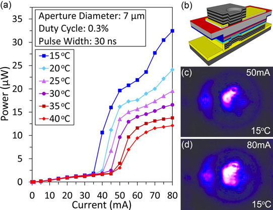
Figure 3: (a) Dependence of time-average output power on current for VCSEL for range of stage temperatures. (b) Schematic cross-section of completed VCSEL. Near-field images of VCSEL at (c) 50mA and 15°C and (d) 80mA and 15°C.
The laser light was not centered in the 7μm-diameter aperture – possibly the result of “inhomogeneity in material composition, surface morphology, local cavity length, current spreading, or transverse optical confinement,” according to the researchers.
The polarization of the emitted laser light at 20°C with 60mA injection was found to be 100% in [1-210] a-direction. The researchers took care to filter out light from spontaneous emission from the polarization measurements.
With c-plane laser diodes, some devices have been reported with 80% polarization – however, in general, the light from c-plane devices should be randomly polarized across an array due to the circular symmetry of the band structure of c-plane devices. By contrast, m-plane MQW devices exhibit a splitting occurs in the top valence band levels due to unbalance biaxial stress. This leads to stronger coupling to electric fields polarized along the a-direction.