Researchers in Singapore have reported high-frequency performance of gallium nitride (GaN) indium aluminium nitride (InAlN) high-electron-mobility transistors (HEMTs) on silicon substrates, including the first noise measurements [S. Arulkumaran et al, IEEE Electron Device Letters, published online 13 August 2014]. The team from Nanyang Technological University and the A*STAR (Agency of Science, Technology and Research) organization believe such devices are good candidates for low-noise and high-linearity receiver circuit applications.
The product of the unilateral power gain cut-off and gate length is the "highest ever reported for InAlN/GaN HEMT on Si substrate", according to the researchers. Alternative substrates for GaN HEMTs are silicon carbide (SiC) or sapphire.
The HEMT heterostructures were grown on high-resistivity silicon (111) substrates using metal-organic chemical vapor deposition (MOCVD). The nucleation layer of 100nm AlN was followed by a 1000nm GaN buffer, 1nm AlN spacer and 9nm In0.17Al0.83N barrier. The InAlN composition gives a lattice match to that of GaN. The InAlN/AlN/GaN interface results in a two-dimensional electron gas (2DEG) channel in the GaN buffer with mobility of 759cm2/V-s and carrier concentration of 2.74x10¹³/cm2.
HEMT fabrication began with mesa isolation through a plasma etch process. The ohmic contacts consisted of annealed titanium/aluminium/nickel/gold. The T-gate of nickel/gold had a 0.17μm footprint/gate length (Lg) and 0.5μm head. The gate width was 2x75μm. The source-gate and gate-drain separations were 0.8μm and 1.7μm, respectively. Passivation was provided by plasma-enhanced chemical vapor deposition (PECVD) of silicon nitride.
The maximum current density of the device was 1320mA/mm at 1V gate potential. The maximum extrinsic transconductance was 363mS/mm. The researchers comment: "The observed current density is almost double than that of similar AlGaN-barrier thick GaN HEMTs (800mA/mm)."
In frequency measurements, the cut-off (fT) was found to be 64GHz at -2.4V gate and 6V drain biases. The unilateral power gain cut-off (fmax(U)) was 72GHz. The maximum stable gain fmax(MSG) was 106GHz. The researchers add: "The product fmax(U)xLg=12.24GHz-μm is the highest ever reported for InAlN/GaN HEMT on Si substrate." In InAlN-barrier HEMTs on silicon carbide, a product of 25GHz-μm has been achieved, possibly due to better 2DEG mobility or lower parasitic effects.
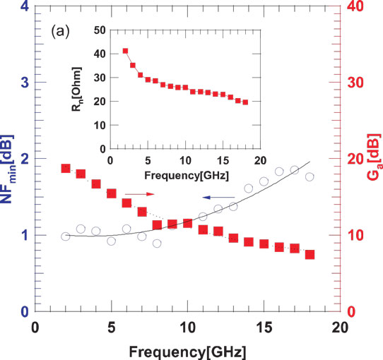
Figure 1: (a) NFmin and Ga versus frequencies (2–18 GHz).
Noise performance was measured between 2GHz and 18GHz with a drain bias of 4V and gate potential of -2.25V (Figure 1). The minimum noise figure (NFmin) measurements at 10GHz and 18GHz were 1.16dB and 1.76dB, respectively. The corresponding associated gain (Ga) readings were 11.54dB and 7.5dB. The researchers write: "The obtained NFmin at 10GHz and 18GHz are comparable to the reported values for AlGaN/GaN on Si substrate with the same gate length. The measured NFmin of our devices at 18GHz is comparable to the NFmin of InAlN/GaN on SiC and AlN/GaN on Si substrate (see Table 1)."
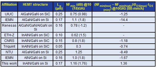
Table 1:
In the lower-frequency 2-8GHz range the Singapore device demonstrated slightly high NFmin values and some variation in performance that could be attributed to shot-noise effects from the gate leakage currents associated with the Schottky-based gate structure. Metal-insulator-semiconductor gate stacks would reduce leakage, hopefully reducing the noise in this lower range.
The noise figure variation (NFmin(low) – NFmin(high))/(IDS(max)-IDS(min)) of 1.36dB-mm/A at 10GHz and 1.67dB-mm/A at 18GHz over the drain current range 100mA/mm-636mA/mm was smaller than found by other groups producing AlN/GaN HEMTs and AlGaN/GaN HEMTs with similar gate lengths on Si substrate (Figure 2). However, short-gate InAlN/GaN HEMTs on SiC show smaller variation, due presumably to the use of field plates and ohmic contact re-growth to reduce access resistance.
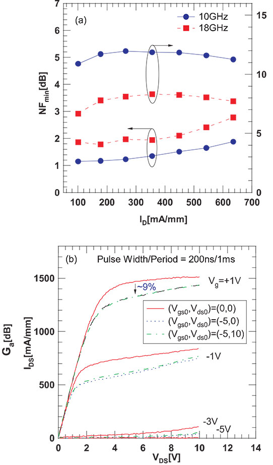
Figure 2: (a) Variation of NFmin and Ga over drain current (ID) at 10GHz and 18GHz. (b) Pulsed drain-source current-voltage (IDS–VDS) characteristics for InAlN/GaN HEMTs on Si substrate.
The researchers also assessed current collapse under gate-lag and drain-lag pulsed bias conditions. The collapse was 9% in both cases. The researchers say that the gate-lag current collapse is better and the drain-lag collapse is comparable to previously reported measurements on InAlN/GaN HEMTs on sapphire substrates. The reduced collapse effect is related to the lattice-matched InAlN barrier and optimized silicon nitride passivation, according to the team.


