Researchers based in the USA and Korea have found "an unequivocal correlation between the onset of high injection and the onset of the efficiency droop" of gallium indium nitride (GaInN) light-emitting diodes (LEDs) [David S. Meyaard et al, Appl. Phys. Lett., vol102, p251114, 2013].
The researchers from Rensselaer Polytechnic Institute, Chonbuk National University, and Samsung Electronics, use their observations to suggest that an electric field develops in the p-type region of the device that sweeps electrons out of the active light-emitting region despite high barriers provided by aluminium gallium nitride (AlGaN) layers that are supposed to act as "electron-blocking layers" (EBLs). The electron leakage from the active region results in degradation of efficiency.
The 440nm blue LED material was grown using metal-organic chemical vapor deposition (MOCVD). The active region consisted of five indium gallium nitride (InGaN) wells separated by GaN barriers. The structure includes an Al0.15Ga0.85N EBL deposited on a 6nm GaN spacer from the last InGaN well. The LEDs were bonded to a silicon wafer and the sapphire growth substrate removed by laser lift-off. The exposed N-face of the nitride structure was roughened to improve light extraction. The LED wafer was diced into unpackaged 1cm x 1cm chips.
Low-level injection describes the condition where conduction by the majority carrier dominates in the quasi-neutral region of a doped semiconductor. In nitride semiconductor LEDs, violation of low-level injection is accompanied by a significant voltage drop across the electron-blocking layer and the p-GaN contact quasi-neutral region.
The researchers determined the onset of high-level injection in the diode as being when the low-level exponential dependence of current on voltage transitions to a linear behavior. This point was found by considering the slope of the logarithm of current with voltage, which takes an abrupt downward path at the transition.
The researchers correlated the onset of high-level injection with the peak efficiency current of the light output over the temperature range 200-450K.
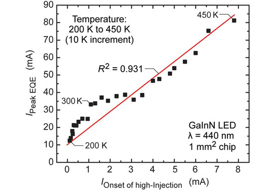
Figure 1. Current at the onset of high injection, correlated with current of peak efficiency for GaInN LED in temperature range 200 400K.
The reason for studying temperature dependence is that the various efficiency-sapping mechanisms have different behaviors. For example, Shockley?Read?Hall recombination of electrons through mid-gap impurity levels to the valence band is less of a problem at low temperature. By contrast, the desired radiative recombination of electrons and holes into photons is enhanced at cryogenic temperatures. Electron leakage into the p-GaN region is found to be greater at 200K than at room temperature (~300K).
The factors combine to reduce the peak efficiency at high temperature. It is also found that position of the peak shifts up in current as the temperature increases. A further observation is that the droop after the peak is sharper near 200K. Such an increase in the droop effect at cryogenic temperatures has been reported by others.
Plotting the onset currents of external quantum efficiency (EQE) droop against high-level injection (Figure 1), the researchers find a linear trend with strong correlation (R2 of 0.931). The peak EQE comes at currents about an order of magnitude (~10x) higher than the high-level injection point.
The researchers write: "We propose that the voltage associated with the current difference is required to build up an electric field in the EBL and p-type GaN region. That is, at the onset of high injection, the electric field in the p-type region is negligible; it takes an additional incremental voltage drop over this region to generate an electric field that will initiate the transport of electrons by drift (rather than diffusion)."
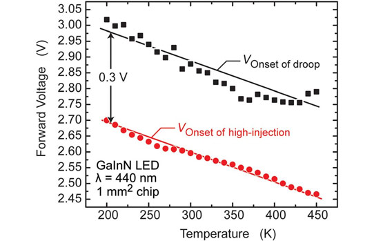
Figure 2. Voltage at the onset of high injection and voltage at onset of efficiency droop (peak-efficiency point) as function of temperature.
Looking at the forward voltage at peak EQE and the onset of high-level injection over the temperature range (Figure 2), the researchers find a roughly constant difference of 0.3V. The researchers believe that a portion of this voltage drop is made over the EBL and p-GaN contact materials.
The researchers comment: "The parallel nature of the two lines constitutes evidence that the efficiency droop is directly linked to the onset of high-injection. As an electric field builds up in the EBL and p-type GaN, electrons are extracted out of the active region, thereby causing the efficiency droop."
Although the electron concentration in the EBL is of the order of 0.1% (~1/1000) of that in the last QW, the researchers believe that the electric field reduces the lifetime for the sweeping out of electrons from the p-type EBL and GaN regions (τDL) to values significantly smaller than the radiative lifetime in the quantum well (τrad~10nsecs). This can enhance the fraction of electrons that leak out of the QW to replace those swept from the p-type regions by the electric field (Figure 3).
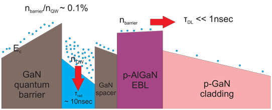
Figure 3. Schematic conduction-band diagram of GaInN LED structure in high-level injection regime leading to electron escape from active region.
APSYS simulations suggested that τDL could be of the order of tens of picoseconds at the onset of droop, where the average electric field across the p-type regions has increased by about 3kV/cm above that of the point of high-level injection. The simulations included an Auger recombination coefficient of 10-34cm6/sec that is much smaller than the 10-29cm6/sec needed to explain droop effects in nitride semiconductors.
The 10-34cm6/sec coefficient is that expected from first-principles calculations of direct Auger recombination, where energy from electron-hole recombination is converted to kinetic energy of a conduction-band electron or valence-band hole. Some theorists have found ways to enhance the Auger coefficient through resonance or excited-state contributions to give values closer to that needed to explain droop.
The US/Korean researchers believe that, apart from the expected smallness of the Auger coefficient, the mechanism also offers a poor explanation because it cannot describe the larger droop at cryogenic temperatures, and the appearance of droop in other material systems such as AlGaInP LEDs, among other features.
By contrast, "these key characteristics can be explained, qualitatively as well as quantitatively, by the drift-leakage model", they write.


