At the 18th International Conference on Crystal Growth and Epitaxy (ICCGE-18) in Nagoya, Japan (7-12 August), analytical and imaging instrument maker Nanophoton Corp of Osaka, Japan has introduced the RAMANdrive wafer analyzer for a wide range of applications in the semiconductor market.
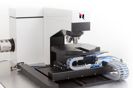
With sub-micron resolution, RAMANdrive provides stress, polytype, defect distribution etc in three dimensions using Nanophoton's most powerful Raman imaging technology. The dedicated 300mm stage was developed for accurate and safe analysis of the whole wafer, while the Raman Imaging System provides high-performance data.
Raman imaging provides comprehensive data about stress, polytype, impurity or contamination non-destructively in all three dimensions, notes president/CEO Michael Verst. "In combination with our dedicated 300mm wafer stage, I strongly believe that our RAMANdrive will be a powerful tool especially for QA/QC as well as development work. It will substantially improve the yield ratio, but also accelerate the development of new materials etc," he adds. "Nanophoton invested a substantial amount of efforts in the development, and during all the time we worked closely with related experts to meet the requirements of our customers in the semiconductor industry."
The unique features of RAMANdrive include the following:
1.The unique Nanophoton Stage Navigation System features what is said to be easy and fast operation by implementing data from the regular inspection system and using it to move the wafer safely and with high accuracy to all positions of interest for detailed analysis.
2.RAMANdrive uses high-quality dark-field microscopy to easily localize and identify particles even smaller than 100nm. Analysis is done by high-performance Raman spectroscopy and provides detailed analysis of the composition of the material.
3.High-quality confocal optics gives RAMANdrive high-performance 3D Raman imaging capability. Stress distribution and polytype distribution can be clearly visualized in 3D with submicron resolution.


