Researchers at Hokkaido University and Japan Science and Technology Agency—PRESTO have reported surrounding-gate transistors (SGTs) using compound semiconductor core–multishell (CMS) nanowire (NW) channels on silicon that demonstrate greatly enhanced on-state current and transconductance while keeping good gate controllability [Katsuhiro Tomioka et al, Nature, published online 1 August 2012].
The researchers comment: ''These devices provide a route to making vertically oriented transistors for the next generation of field-effect transistors and may be useful as building blocks for wireless networks on silicon platforms.''
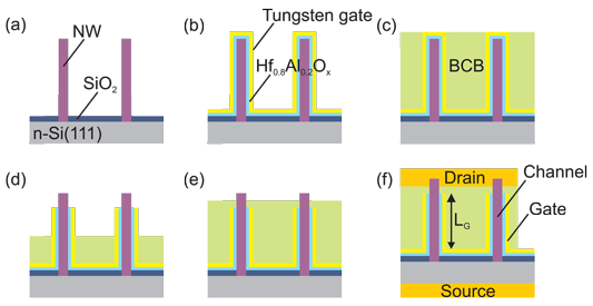
Figure 1. Device fabrication processes: (a) NW growth. (b) ALD of HfAlOx and sputtering of W-gate metal. (c) Spin-coating of BCB polymer. (d) RIE of BCB, gate oxide and W metal. (e) Spin-coating of BCB and RIE etch-back for electrical separation layer formation. (f) Drain and source metal evaporation.
The nanowires were grown vertically on Si(111) substrates using metal-organic chemical vapor deposition (MOCVD). The SGTs were constructed using atomic layer deposition (ALD) of hafnium aluminium oxide (Hf0.8Al0.4Ox) dielectric, sputtering of tungsten gate metal, spin-coating of benzocyclobutene (BCB), reactive ion etch-back (RIE) to define gate length, further spin-coating/RIE to isolate drain from gate metal. Further processing resulted in the deposition of source and drain contacts etc.
SGTs were formed from different types of nanowires. First, pure indium gallium arsenide (InGaAs) NW-SGTs were produced with an on/off current ratio of 106, sub-threshold swing (SS) of 82mV/dec and drain-induced barrier lowering (DIBL) of 45mV/V.
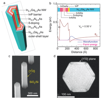 Figure 2. a, Schematic of indium gallium arsenide/indium phosphide/indium aluminum arsenide/indium gallium arsenide (InGaAs/InP/InAlAs/InGaAs) CMS nanowires on Si. The InAlAs layer is δ-doped with Si. b, Simulated band diagram of the MD-CMS nanowire at 0.5V gate potential. Without gate bias, the carrier wavefunction is confined in the outer InGaAs shell layer. c, Typical SEM image showing vertical MD-CMS nanowires on Si. Average diameter and height of nanowires are 180nm and 1.2μm, respectively. d, Electron micrograph showing representative cross-section of a CMS nanowire with total diameter of 180nm.
Seeking improvement from this base, the researchers developed modulation-doped core–multishell (MD-CMS) nanowires consisting of layers of different compound semiconductor and doping applied to an InGaAs core using metal-organic sources (Figure 2). This raised the on/off ratio to 108, lowered SS to 75mV/dec, and DIBL to 35mV/V (Figure 3). The maximum drain current was 0.45mA/μm and the peak transconductance was 1.42mS/μm with the gate 0.5V above threshold (0.38V) and the drain biased at 0.5V.
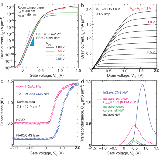
Figure 3. Performance of SGT using InGaAs/InP/InAlAs/InGaAs CMS nanowire channels on Si. a, Transfer characteristics of SGT with gate length 200nm and gate-drain distance 50nm. SS is 75mV per decade and DIBL is 35mV/V. Dashed line indicates physical limit of SS (60mV per decade at room temperature). b, Output characteristics of an InGaAs CMS nanowire SGT. c, Capacitance/gate voltage curve of InGaAs nanowire (pink circles) and InGaAs CMS nanowire (blue circles). Capacitances are measured values divided by number of nanowires (250 for InGaAs nanowires and 512 for InGaAs CMS nanowires). Measurement frequency is 1MHz. d, Transconductance of SGTs using InGaAs nanowires (black), InGaAs/InAlAs core–shell nanowires (green), MD-CMS nanowires with gate-drain distance of 1μm (pink; IEDM) and latest MD-CMS nanowires (blue). Drain bias 0.5V.
The researchers comment: ''The very large increase in ID and Gm, together with the steep SS, indicates that the CMS multilayers acted as a modulation-doped, high-electron-mobility structure while maintaining good controllability of the surrounding-gate structure. These results are superior to those from devices made from similar materials and with similar dimensions.''
In December 2011, the researchers presented InGaAs and multi-shell nanowire transistors with similar on/off ratios, but worse SS and DIBL values (97mV/dec, 160mV/V, respectively) at the International Electron Device Meeting last year (IEDM 2011, Semiconductor Today report, February 2012, p88). Also, the earlier devices had lower drain currents and transconductance.
More recently, the team presented tunneling field-effect transistors based on NWs at VLSI (ST report June/July 2012, p98). Due to the different device structure the SS values were as low as 21mV/dec with on/off ratios of 106. The tunneling structure allows SS below the room-temperature theoretical minimum of 60mV/dec for more traditional structures, such as the SGTs presented here.


