Researchers in Germany have developed two-dimensional hole gas (2DHG) gallium nitride (GaN) channel structures with record mobility [B Reuters et al, J. Phys. D: Appl. Phys., vol47, p175103, 2014]. Mobility for 2DHGs in GaN is usually around 10cm2/V-s. Two-dimensional electron gas (2DEG) mobility is much higher, at around 1000cm2/V-s.
The research by RWTH Aachen University, Forschungszentrum Jülich GmbH, Jülich Aachen Research Alliance (JARA)-Fundamentals of Future Information Technologies, and Aixtron SE resulted in one sample with a 2DHG mobility as high as 43cm2/V-s.
The researchers also produced p-type heterostructure field-effect transistors (p-HFET). Some of these devices demonstrated depletion-mode (normally on) operation. Other devices worked in enhancement mode, giving normally-off behavior that is desired for low power consumption.
Producing p-type hole conductivity in nitride semiconductors is inhibited by background impurities such as silicon or oxygen that act as donors in GaN, meaning that unintentionally doped material is n-type.
The researchers in Germany used an aluminium indium gallium nitride (AlInGaN) back-barrier and magnesium doped bulk p-GaN above the unintentionally doped channel layer. By varying the composition of the back-barrier, different polarization fields could be set up, allowing 2DHGs with different properties to be realized. The upper p-GaN layers were designed to compensate for the typical n-type behavior of the unintentionally doped (uid) GaN channel layer.
The epitaxial structures (Figure 1) were grown on 2-inch c-plane sapphire in an Aixtron horizontal-flow metal-organic vapor phase epitaxy reactor. The surface temperature and growth rate were carefully controlled using spectroscopic measurements over the wavelength range 276-775nm from a LayTec tool, in combination with true-temperature pyrometer data.
Figure 1: (a) Schematic of nitride semiconductor stack grown by MOVPE. (b) Corresponding schematic of band structure.
Five samples were produced with various AlInGaN compositions for the back-barrier. The composition variation was created through different growth temperatures and trimethyl-Al/Ga precursor flow ratios. The aim was to achieve different spontaneous and piezoelectric (strain-dependent) polarizations, giving control over the contrast with GaN (Table 1).
Table 1: Sample identification with, respectively, growth surface temperature, precursor Al-to-Ga molar gas phase ratio, compositions determined by Rutherford backscattering spectrometry (RBS) and high-resolution x-ray diffraction (HRXRD), spontaneous and piezoelectric polarization, and polarization difference with GaN.
Sample TS (?C) TMAl/TMGa ratio Al (%) In (%) Ga (%) ?Psp (C/m2) ?Ppz (C/m2) ΔP (C/m2) A 820 2.4 54 4 52 0.058 0.012 0.036 B 815 1.2 42 3 55 0.052 0.009 0.027 C 807 0.6 25 2 73 0.044 0.004 0.014 D 798 0.4 20 2 78 0.041 0.003 0.010 E 793 0.2 14 2 84 0.039 0.001 0.006
The more heavily doped p++-GaN surface layer was aimed at ohmic contact formation. The magnesium acceptors were activated with a 20-minute 700°C anneal process in nitrogen.
Test structures, including a heterostructure field-effect transistor (HFET), were produced with annealed nickel/gold ohmic contacts, molybdenum Schottky gates, and gate and access region recessing through the surface p++-GaN and graded p+-GaN layers with a digital etch process. The gate recessing reduced gate leakage by about four orders of magnitude, according to the researchers.
Hall measurements gave 2DHG densities of between 2x10¹³/cm2 and 6x10¹¹/cm2. A record hole mobility of 43cm2/V-s was achieved for sample C at 1.3x10¹²/cm2 carrier density. However, sample C also suffered from a wider spread of results compared to the other samples. Overall, sample C had a median mobility of 30cm2/V-s and 2.2x10¹²/cm2 carrier density.
HFETs with 1μm gate length and 7nm recess were fabricated. Sample A produced HFETs with depletion-mode/normally-on behavior.
The drain current reached more than 40mA/mm for a negative gate potential of ?3V and drain bias 10V. A positive gate potential of 3.5V gave an off-current of 0.01mA/mm, resulting in an on/off ratio of more than 1000. Higher drain currents of more than 100mA/mm have been achieved in 2DHG HFETs, but these devices have only achieved on/off ratios of around one order of magnitude.
The peak transconductance was 9mS/mm. Frequency measurements resulted in a cut-off frequency (fT) of 206MHz and maximum oscillation (fmax) of 640MHz.
Enhancement-mode performance was achieved using sample E with a low polarization difference (Figure 2). The maximum drain current and peak transconductance at 5V drain bias were 0.7mA/mm and 0.2mS/mm. These low values were offset by an even greater reduction in off-current, giving an on/off ratio 108, "the best value ever published for p-channel transistors," according to the researchers.
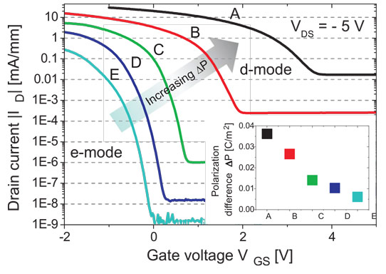
Figure 2: Absolute drain current versus gate voltage. Threshold voltage shifts from negative values (enhancement-mode) to positive values (depletion-mode) with increasing ΔP. Inset: calculated ΔP values for each sample.
The researchers say that the on/off performance of the enhancement-mode transistor shows "great potential of these devices for applications like complementary III-nitride logics for harsh environments".


