Researchers in the USA at BAE Systems and Purdue University have developed atomic layer deposited (ALD) aluminium oxide as passivation for nitride semiconductor high-electron-mobility transistors (HEMTs) [Dong Xu et al, Electron Device Letters, published online 22 April 2013].
Nitride HEMTs allow higher power density and higher-efficiency amplification at high frequency. However, current collapse with pulsed signals needs to be dealt with. One technique is to add field plates that can manipulate electric fields in nitride semiconductor transistors, reducing the effect of interface traps. However, these field plates add parasitic capacitance that impacts frequency and gain performance.
Another approach is to tackle the dangling bonds that create interface traps through passivation layers.
The epitaxial structure for the BAE/Purdue HEMTs was realized using metal-organic chemical vapor deposition (MOCVD) on semi-insulating silicon carbide (SiC) substrates. Aluminium nitride (AlN) was used as a nucleation layer. Part of the gallium nitride (GaN) buffer was iron doped to give a semi-insulating layer below the undoped GaN buffer. The structure was completed with an undoped aluminium gallium nitride (AlGaN) barrier and 2nm GaN cap.
Before the transistor formation the wafers were cleaned in acetone, methanol and isopropanol to remove organic residues and in ammonia solution to strip surface oxide layers. The aluminium oxide (Al2O3) layer was applied by atomic layer deposition in an ASM F-120 system.
The process sequence included ramp-up to 300°C and oxide self-cleaning with trimethyl aluminium (TMA). The Al2O3 passivation layer was built up by alternating pulses of TMA and water (H2O) precursors in nitrogen carrier gas. The growth rate was 0.86Å/cycle.
One aim of the cleaning steps was to unpin the Fermi level by removing oxides on the epitaxial structure that can form trap states at the interface with the gate. The researchers estimate the as-grown interface trap density for their Al2O3/GaN cap at between 1011/cm2-eV and 1012/cm2-eV. This can be reduced to less than 1011/cm2-eV by a post-deposition anneal.
Comparison wafers were also produced with a more conventional silicon nitride (SiN) passivation applied with plasma-enhanced chemical vapor deposition (PECVD) at 250°C and an ammonia plasma pre-treatment.
The passivated material was used to create 200nm-long T-gate HEMTs with mesa isolation achieved using inductively coupled plasma etch. The ohmic source-drain contacts consisted of annealed titanium/aluminium/gold.
One effect of the Al2O3 layer is to reduce parasitic resistance due to the improved interface between passivation and GaN cap. This increases the 10V-drain-bias maximum drain current and extrinsic peak transconductance by 10% and 8%, respectively, over the values for SiN passivation. In addition, the subthreshold drain current is reduced by an order of magnitude in the Al2O3 device.
The subthreshold current is attributed to gate leakage, which in the Al2O3 device is reduced due to the improved interface leading to better performance of the Schottky gate under reverse bias.
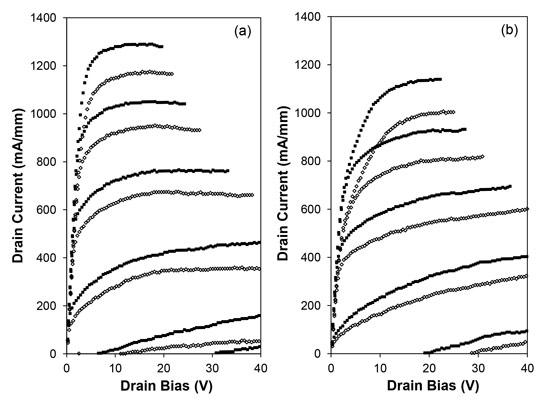
Figure 1: Pulsed current-voltage (IV) characteristics for 200nm-long T-gate GaN HEMTs with PECVD SiN (open symbols) and ALD Al2O3 passivation (solid symbols). Devices were measured at quiescent points of (a) 0V gate and drain and (b) -5V gate and 30V drain. The gate for the top curves was 1V, and the others represent -1V steps.
Performance under pulses with 200nsec width and 2msec separation was tested at different quiescent points (Figure 1). With the quiescent gate and drain bias at 0V, the maximum drain current was 10% better in the Al2O3 device. A ‘deep’ quiescent point of -5V gate and 30V drain gave an even better maximum drain current performance boost of 20% to the Al2O3 passivated HEMT. The pulsed performance is also more uniform across the 3-inch wafers that contain the Al2O3 HEMTs: the maximum current standard deviation was 11mA/mm at the zero quiescent point and 20mA/mm for the deep quiescent point, compared with 49mA/mm and 54mA/mm, respectively, for the SiN-passivated HEMT.
The researchers comment: “The improved uniformity and consistency of pulsed-IV performance with the use of ALD Al2O3 layer passivation layer would certainly contribute to higher yield of MMICs based on these devices, making it a more manufacturing friendly technology.”
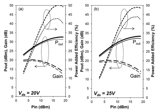
Figure 2: Output power, associated power gain, and power-added efficiency as a function of drive for 200nm 4x100μm HEMTs passivated with PECVD SiN (thin lines) and ALD Al2O3 (thick lines) at 10GHz. Devices were biased at drain current of 200mA/mm and drain voltage of (a) 20V and (b) 25V.
The frequency performance of the two device types were similar, with a cut-off frequency (fT) of 54-55GHz and maximum oscillation (fmax) of 117-120GHz at 20V drain. However, the 10GHz continuous wave (CW) power performance (Figure 2) at 20V drain of the Al2O3 device was 30% better in terms of maximum output (4.55W/mm versus 3.5W/mm). Also, the power-added efficiency (PAE) was better by about 8%. Increasing the drain bias to 25V slightly reduced the enhancement to 27% for maximum power output and 5% for PAE.


