Fangliang Gao and Guoqiang Li of South China University of Technology have developed a technique to grow high-quality indium gallium arsenide (InGaAs) on gallium arsenide substrates using an ultrathin amorphous buffer [Appl. Phys. Lett., vol104, p042104, 2014].
The researchers see their process as having applications to tandem solar cells, replacing the usual germanium layers in these structures. The germanium layer can lead to a large mismatch in photocurrent: in the case of gallium indium phosphide/indium gallium arsenide/germanium (GaInP/InGaAs/Ge, 1.84eV/1.4eV/0.67eV bandgaps) multi-junction cells, the germanium photocurrent density is around two times that in the other two layers. Photocurrent mismatch leads to degradation of conversion efficiency.
A 1eV bandgap bottom layer would solve the mismatch problem and In0.3Ga0.7As has a 1eV bandgap. However, such InGaAs films have a lattice mismatch of 2.3% with GaAs substrates. The usual approach to bridge such mismatches is to use compositionally graded buffer layers. “However,” the researchers write, “it is always a big challenge to accurately control the composition, the thickness, and the crystal quality of each sublayer for the buffer layers, not to mention the tedious procedures to grow so many sublayers.” As-grown In0.3Ga0.7As films on GaAs with compositionally graded buffers tend to have worse-than-expected quality.
Gao and Li grew their InGaAs films on semi-insulating GaAs (111) substrates using molecular beam epitaxy (MBE). The process began with an In0.6Ga0.4As buffer layer grown on the substrate at 380°C. Different buffer thicknesses - 10nm, 4nm, 2nm, 1nm, 0nm - were tried to optimize the quality of the top 500nm In0.3Ga0.7As grown at 540°C.
The resulting epitaxial structures were studied using high-resolution x-ray diffraction (HRXRD), high-resolution transmission electron microscopy (HRTEM), scanning electron microscopy (SEM), and atomic force microscopy (AFM).
The 10nm buffer layer was found to be amorphous due to the low growth temperature, the large 4.3% lattice mismatch with the GaAs substrate, and the large indium content, which has a much larger atomic radius (142pm) than gallium (122pm) or arsenic (119pm). With 10nm buffer, the top InGaAs layer is polycrystalline, as revealed using halo selected-area electron diffraction (SAED) performed with the TEM system.
Reducing the amorphous buffer to 4nm gave a single-crystalline In0.3Ga0.7As layer, although there was a large density of dislocations. The HRXRD rocking curve full-width at half maximum (FWHM) of the In0.3Ga0.7As (111) layer was 980arcsec.
Further improvement came with decreasing the buffer thickness to 2nm. “The as-grown In0.3Ga0.7As epitaxial film is almost dislocation-free compared with the two previous samples with thicker In0.6Ga0.4As buffer layers,” the researchers write. The etch pit density, which reflects dislocation densities, was 3.3x10⁶/cm2.
High-resolution x-ray reciprocal space mapping indicated that the lattice parameter of the film was 0.57713 nm, which is very close to the fully relaxed value of 0.57749 nm (Figure 1). The XRD rocking curve FWHM was 108arcsec.
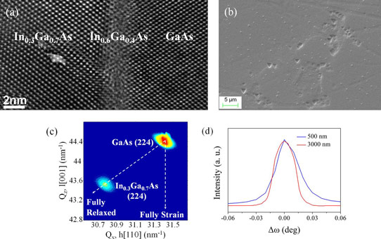
Figure 1: (a) Cross-sectional HRTEM image, (b) SEM image of etched surface, and (c) high-resolution reciprocal space mapping for (224) diffraction of 500nm-thick In0.3Ga0.7As on 2nm-thick In0.6Ga0.4As/GaAs heterostructure and (d) XRD rocking curves of 500nm (blue line) and 3000nm (red line) In0.3Ga0.7As (111) films grown on 2nm In0.6Ga0.4As amorphous buffer.
A comparison In0.3Ga0.7As film was grown on a four-step-graded-composition InxGa1-xAs buffer layer (x ~ 0.09, 0.18, 0.27, and 0.33, respectively).
AFM studies on 5μmx5μm fields gave root mean square (RMS) roughness values of 1.1nm and 1.2nm for In0.3Ga0.7As grown on 2nm amorphous In0.4Ga0.6As and on four-step graded buffers, respectively (Figure 2). Also, the XRD rocking curve FWHM for the film on four-step-graded buffer was 116arcsec, compared with 108arcsec for In0.3Ga0.7As on 2nm amorphous In0.4Ga0.6As.
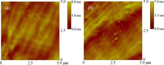
Figure 2. AFM images (5μmx5μm) of In0.3Ga0.7As epitaxial layers grown on GaAs substrates with buffer structures of (a) 2nm amorphous In0.6Ga0.4As and (b) four-step-graded-composition layer.
The four-step-graded buffer process also gave similar values for etch-pit density and lattice constant of 3.6x10⁶/cm2 and 0.57706nm, respectively.
The researchers comment: “Evidently, the proposed approach is at least competitive, if not better than the usually adopted way using step-graded-composition buffer layers. Given its simplicity, this approach shows a high potential as a replacement for the routine composition-graded buffer layer currently used to produce high-quality 1eV solar cell junctions.”
The researchers believe that the 2nm amorphous layer traps threading dislocations and introduces a high density of defects at the In0.6Ga0.4As/GaAs interface reducing residual strain, thus inhibiting nucleation of dislocations in the In0.3Ga0.7As epi-layer.
The researchers write: “The ultrathin amorphous In0.6Ga0.4As buffer layer is acting like an ‘elastic layer’ between In0.3Ga0.7As epi-layer and GaAs substrate. This elastic layer contains a high density of point defects. As a result, dislocations can be easily nucleated. At the same time, point defects can promote dislocation glide and consequently block the penetration of dislocations into the following In0.3Ga0.7As epi-layer. Clearly, this amorphous elastic layer can efficiently release misfit strain and trap dislocations.”
Increasing the thickness of the In0.3Ga0.7As film to 3000nm reduced the XRD FWHM to 90arcsec, indicating even better crystallinity. The researchers see this as indicating that their process can provide “favorable conditions for the subsequent epitaxial growth of In0.3Ga0.7As solar cell layers”.
Reducing the thickness of the amorphous layer below 2nm leads to deterioration in the In0.3Ga0.7As layer with XRD rocking curve FWHMs of 556arcsec and 1292.9arcsec for 1nm and 0nm buffer thickness, respectively.


