AIXTRON SE introduced a 5 x 200mm gallium nitride on silicon (GaN-on-Si) reactor design for its G5 Planetary Reactor metal organic chemical vapor deposition (MOCVD) platform. AIX G5+ comprises special reactor hardware and process design, developed with customers in AIXTRON’s R&D lab.
Any existing G5 system can be upgraded to this latest version.
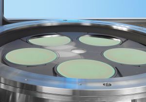
Figure. AIX G5+ offers fully rotationally symmetrical uniformity pattern on five wafers.
Power electronics makers are using GaN-on-Si technology, and future high-brightness light-emitting diodes (HB-LEDs) are in development on GaN-on-Si substrates, noted Dr. Rainer Beccard, VP, marketing at AIXTRON. Recent GaN-on-Si development has occured at Lattice Power, NXP Semiconductors, EpiGaN, Bridgelux, Toshiba, and Nitronex, among other semiconductor and LED makers.
GaN-on-Si offers high performance on a lower-cost substrate than sapphire. “Wafer size and material plays a crucial role when it comes to cost-effective manufacturing processes, and thus the transition to 200mm standard silicon wafers is a logical next step on the manufacturing roadmaps,” said Beccard.
The GaN-on-Si reactor was designed for high uniformity and yield. It was developed via simulations, which guided the “fundamentally new” hardware design in the 5 x 200mm configuration.
Select AIXTRON customers are using the AIX G5+, reporting fully rotationally symmetrical uniformity pattern on all five 200mm wafers, which are standard-thickness silicon substrates. These trials also show controlled wafer bow behavior.


