Xidian University has developed a nitride semiconductor field-plated metal-insulator-semiconductor high-electron-mobility transistor (FP MIS-HEMT) with ‘negligible’ current collapse, along with high maximum current and enhanced breakdown voltage performance [Mao Wei et al, Chin. Phys. Lett., vol30, p058502, 2013]. The device uses silicon nitride (SiN) as gate insulation and passivation to achieve these results.
Current collapse is a serious problem in nitride HEMTs, observed in pulsed operation in comparison with direct current (DC) performance. Since transistors tend to be operated with varying bias conditions, such performance degradation must be minimized.
The nitride layers of the FP MIS-HEMT (Figure 1) were grown using metal-organic chemical vapor deposition (MOCVD) on c-plane sapphire. The barrier layer consisted of indium aluminium nitride (In0.15Al0.85N), which is nearly lattice matched to the underlying gallium nitride (GaN).
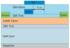
Figure 1: Schematic of FP MIS-HEMT.
The GaN and AlN layers were grown at 940°C/40Torr. The InAlN was constructed using a pulse approach at the lower temperature of 760°C/200Torr as a series of short-period AlN/InN superlattices to improve indium incorporation. The nitride semiconductor structure had a two-dimensional electron gas (2DEG) with 1.49x10¹³/cm2 carrier density and 1503cm2/V-s mobility.
Device fabrication began with mesa isolation reactive ion etching and deposition of ohmic titanium/aluminium/nickel/gold source-drain electrodes separated by 3.5μm.
The first layer of 7nm silicon nitride (SiN) was then deposited using plasma-enhanced chemical vapor deposition (PECVD). The gate was then created with a nickel/gold/nickel structure at a distance of 0.7μm from the source terminal. The gate was 0.6μm long and 100μm wide. Another 55nm of SiN was deposited, followed by a titanium/gold gate field plate (FP) with an effective length of 0.3μm.
A comparison HEMT was also produced without a field plate or SiN insulation/passivation.
One effect of the structure is to reduce gate leakage currents. Under a reverse bias of -15V, the leakage is suppressed by almost one order of magnitude. At forward biases of 2V, the leakage is suppressed by more than five orders of magnitude. At 5V forward bias, the leakage was 0.02mA/mm. Breakdown occurred above 5V gate bias, giving an estimated critical field in the SiN of 7.1MV/cm. The field was in line with that achieved with other PECVD SiN films (3-12MV/cm).
The maximum drain current with 10V drain bias was 1211mA/mm (5V gate), compared with 836mA/mm (1V gate) for the comparison HEMT. However, the peak transconductance was reduced to 184mS/mm (318mS/mm in the comparison HEMT) due to the lower electrostatic control of the gate through the SiN layers of the FP MIS-HEMT.
The off-state breakdown characteristics (-8V gate, 1mA/mm gate leakage) were 120V drain bias for the FP MIS-HEMT and 82V for the comparison HEMT. “This improvement is attributed not only to the adoption of the SiN gate dielectric layer to reduce the leakage current but also to the adoption of the FP, which effectively modulates the magnitude of the peak electric field near the drain side of the gate edge and the distribution of the electric field between the gate and the drain,” the researchers write
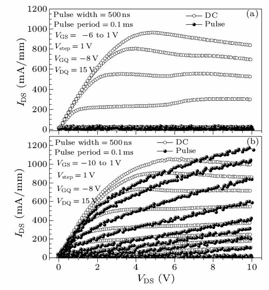
Figure 2: DC and pulsed current-voltage (I V) performances of HEMT (a) and FP-MIS HEMT (b).
Pulsed operation was tested to reveal current collapse effects. The baseline bias was -8V gate and 15V drain. The pulse width was 500nsec with a period of 0.1msec. The current collapse of the comparison HEMT was ‘pronounced’, while the researchers described that of the FP MIS-HEMT as being ‘negligible’ (Figure 2). “These considerable improvements in the current collapse for the FP MIS-HEMT are attributed not only to the passivation effect of the SiN layer on the surface state traps, but also to the modulation of the ionization probability of the traps in terms of the FP,” they write.


