For decades, researchers have tried to harness the unique properties of carbon nanotubes (CNTs) to create high-performance electronics that are faster or consume less power — resulting in longer battery life, faster wireless communication and faster processing speeds for devices like smartphones and laptops. But a number of challenges (such as constraints in CNT sorting, processing, alignment, and contacts) have impeded the development of high-performance transistors made of carbon nanotubes. Consequently, their performance has lagged far behind semiconductors such as silicon and gallium arsenide (GaAs) in computer chips and personal electronics.
Now, led by professors of materials science and engineering Michael Arnold and Padma Gopalan, researchers at University of Wisconsin–Madison have created carbon nanotube transistors that for the first time outperform state-of-the-art silicon transistors, it is claimed, achieving on-state current density 1.9 times higher than silicon transistors (G J Brady et al, 'Quasi-ballistic carbon nanotube array transistors with current density exceeding Si and GaAs', Science Advances vol2 (2016), no9, e1601240).
Specifically, the researchers have fabricated field-effect transistors (FETs) with a density of 47 CNTs μm-1 and a channel length of 100nm, yielding conductance as high as 0.46G0 per CNT. In parallel, conductance of the arrays reaches 1.7mS μm-1, seven times higher than the previous state-of-the-art CNT array FETs made by other methods. Saturated on-state current density is as high as 900μA μm-1, similar to or exceeding that of silicon MOFETs (at an equivalent gate oxide thickness and the same off-state current density) and exceeding the 630μA μm -1 of GaAs pseudomorphic high-electron-mobility transistor (pHEMT) technology.
"This breakthrough in carbon nanotube transistor performance is a critical advance toward exploiting carbon nanotubes in logic, high-speed communications, and other semiconductor electronics technologies," says Arnold. This advance could pave the way for carbon nanotube transistors to replace silicon transistors and continue delivering the performance gains the computer industry relies on, it is reckoned. The new transistors are particularly promising for wireless communications technologies that require a lot of current flowing across a relatively small area. Funding from the US National Science Foundation, the Army Research Office and the Air Force supported the work.
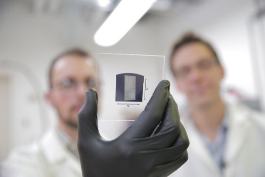
Picture: The UW–Madison engineers use a solution process to deposit aligned arrays of carbon nanotubes onto 1 inch by 1 inch substrates. The scalable and rapid deposition process was used to coat the entire surface of this substrate with aligned carbon nanotubes in less than 5 minutes.
As some of the best electrical conductors ever discovered, carbon nanotubes have long been recognized as a promising material for next-generation transistors. CNT transistors should be able to perform five times faster or use five times less energy than silicon transistors, according to extrapolations from single nanotube measurements. The nanotube's ultra-small dimension makes it possible to rapidly change a current signal traveling across it, which could lead to substantial gains in the bandwidth of wireless communications devices.
But researchers have struggled to isolate purely carbon nanotubes, which are crucial, because metallic nanotube impurities act like copper wires and disrupt their semiconducting properties (like a short circuit).
The UW–Madison team used polymers to selectively sort out the semiconducting nanotubes, achieving a solution of ultra-high-purity semiconducting carbon nanotubes. "We've identified specific conditions in which you can get rid of nearly all metallic nanotubes, where we have less than 0.01% metallic nanotubes," says Arnold.
Placement and alignment of the nanotubes is also difficult to control. To make a good transistor, the nanotubes need to be aligned in just the right order, with just the right spacing, when assembled on a wafer. In 2014, the UW–Madison researchers overcame that challenge by developing the 'floating evaporative self-assembly' technique to give them this control.
The nanotubes must also make good electrical contacts with the metal electrodes of the transistor. Because the polymer used by the UW-Madison researchers to isolate the semiconducting nanotubes also acts like an insulating layer between the nanotubes and the electrodes, the team 'baked' the nanotube arrays in a vacuum oven to remove the insulating layer, yielding excellent electrical contacts to the nanotubes.
The researchers also developed a treatment that removes residues from the nanotubes after they are processed in solution.
"We've shown that we can simultaneously overcome all of these challenges of working with nanotubes, and that has allowed us to create these ground-breaking carbon nanotube transistors that surpass silicon and gallium arsenide transistors," says Arnold.
The researchers benchmarked their carbon nanotube transistor against a silicon transistor of the same size, geometry and leakage current. They are now continuing to work on adapting their device to match the geometry used in silicon transistors, which shrinks with each new generation. Work is also underway to develop high-performance radio frequency amplifiers that may be able to boost a cell-phone signal. While the researchers have already scaled their alignment and deposition process to 1-inch by 1-inch wafers, they are working on scaling the process up for commercial production.
Arnold says researchers can finally exploit the nanotubes to attain performance gains in actual technologies. "There has been a lot of hype about carbon nanotubes that hasn't been realized, and that has kind of soured many people's outlook," he adds. "It has just taken decades of work for the materials science to catch up and allow us to effectively harness these materials."
The researchers have patented their technology through the Wisconsin Alumni Research Foundation.


