IBM Research's Thomas J. Watson Research Center and Northwestern University have developed a technique to grow hexagonal- and cubic-phase gallium nitride (h-/c-GaN) on standard (100) silicon (Si) [Can Bayram et al, Adv. Funct. Mater., published online 1 April 2014].
Although GaN growth on silicon substrates is being widely developed with a view to reduced production costs for high-power and high-frequency transistors and light-emitting devices, usually the non-standard (111) crystal orientation is chosen to give a better lattice match between Si and GaN.
One disadvantage of using (111) silicon is that it reduces the potential for monolithic integration of high performance silicon CMOS with GaN. CMOS transistors on (111) silicon have inferior characteristics.
The researchers also point to cubic-phase GaN having a polarization-free crystal structure. Spontaneous and strain-dependent polarization fields in heterostructures based on hexagonal-phase GaN lead to internal electric fields that degrade performance, particularly in light-emitting applications.
The IBM/Northwestern technique involves etching grooves in the silicon that expose (111) facets that can seed h-GaN growth. When two GaN growth fronts from opposite facets meet, a c-GaN region develops.
The (100) silicon substrate was prepared with an RCA clean and a silicon dioxide (SiO2) mask was created using thermal oxide deposition, 193nm photolithography and reactive-ion etch to expose the Si (100) surface (Figures 1a-c). The next step was to etch the silicon in potassium hydroxide (KOH) solution for a minute to selectively give grooves or trenches with (111) facets (Figure 1d).
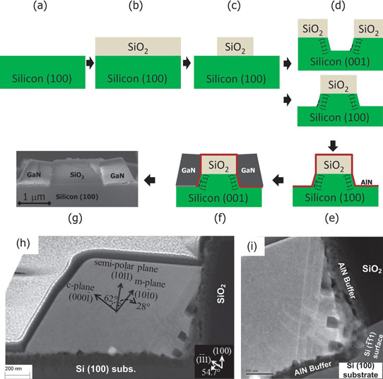
Figure 1: Schematic process flow for silicon (100) substrate preparation and MOCVD growth processes: (a) RCA clean; (b) thermal oxide growth; (c) lithography and reactive ion etch; (d) KOH dip (10%) to give final groove structures: (top) [SiO2 -Si{111}-Si{100}-Si{111}-SiO2 ] or (bottom) [SiO2 -Si{111}-Si{100}]; (e) low-temperature AlN buffer deposition, (f) high-temperature GaN layer deposition. (g–i) Cross-sections of wurtzite phase GaN: (g) SEM and (h) HAADF-STEM view with crystallographic directions, and (i) HAADF-STEM view zoomed in GaN{000 1}-Si{111} interface.
The growth of GaN on an AlN nucleation layer was performed in a metal-organic chemical vapor deposition (MOCVD) system. The AlN was grown at the low temperature of 700°C and was preceded by ammonia-free heat-up and 'prealuminization' steps to remove native oxide and avoid silicon nitride formation. The AlN layer was at least 60nm thick.
The GaN was grown at more than 1150°C, higher than the conventional 1050°C. "Such optimized MOCVD parameters enable a uniform and controlled GaN re-growth over that under conventional condition," according to the researchers.
GaN grown on wide trenches was in the hexagonal wurtzite crystal structure with the Si c-plane growth direction the same as that of the (111) facets of the GaN structure. The researchers found that threading dislocations (TDs) were filtered by m-plane stacking faults so that no TDs were discernable in the topmost GaN, according to cross-sectional transmission electron microscopy (XTEM).
Fast Fourier transform (FFT) electron diffraction analyses also show that the AlN layer is wurtzite on the (111) Si facets but polycrystalline on the (100) Si groove bottom.
Moving from wide trenches to narrower grooves, the GaN grown on facing facets meets and forms in the cubic zincblende structure (Figure 2). Different groove openings of 1000nm, 650nm and 250nm were tested. Where the growth fronts meet, a void forms, along with crystallographic faults.
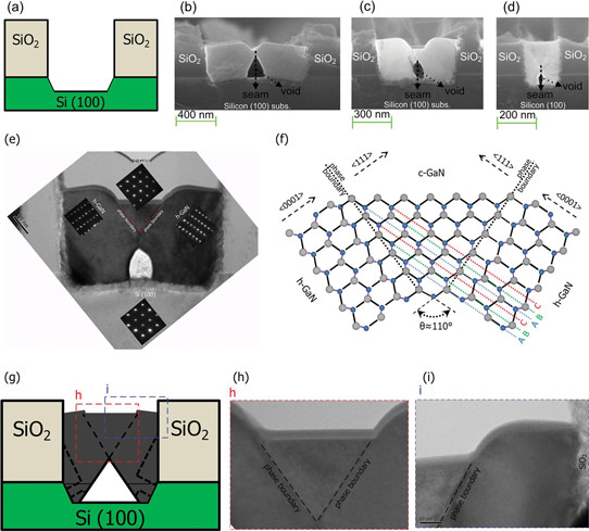
Figure 2: (a) Cross-sectional sketch of [SiO2-Si{111}-Si{100}-Si{111}-SiO2 ] groove structure for GaN re-growth. (b–d) Cross-sectional SEM of GaN grown on grooved Si (100) substrate having openings of (b) 1000 nm, (c) 650 nm, and (d) 250 nm. (e) Cross-sectional bright-field TEM of partially GaN-filled groove structure. FFT diffraction patterns of boxed regions correspond to c-GaN, h-GaN, and Si (100). (f) Cross-sectional sketch depicting wurtzite to cubic phase transition observed in groove. (g) Cross-sectional sketch of partially GaN-filled groove structure. Bright-field TEM images of (h) c-GaN and (i) h-GaN surfaces reveal no threading dislocations.
Electron microscopy showed the faults to be phase boundaries. The researchers report: "Bright-field TEM images in Figure 2 reveal no threading dislocations on both c-GaN and h-GaN surfaces." They further believe that the V-shape phase boundaries circumscribing the cubic phase GaN help to suppress TDs propagating, since the cubic phase growth front is aligned with the Si[100] direction whereas the wurtzite phase growth front is aligned with Si[111].
Micro-Raman spectroscopy, which probes phonon (quantized lattice vibration) characteristics, suggests that the h-GaN and c-GaN regions are stress-free. The researchers believe that the localized epitaxy is the reason for the absence of stress, compared with bulk deposition processes.
Finally, the researchers grew indium gallium nitride multiple quantum wells (InGaN/GaN MQWs) on the c-GaN. 'Intense' photoluminescence peaks were observed from the GaN (~365nm ultraviolet) and InGaN/GaN quantum wells (~420, blue-violet). The GaN peak covered the (~half-maxima) range 360-375nm, and the InGaN/GaN MQW peak was relatively broad (400-450nm). The GaN peak was about 0.8x that of the InGaN/GaN MQW.


