Researchers in Hong Kong and China have claimed the first demonstration of gallium nitirde (GaN) fully vertical p-type-intrinsic-n-type (p-i-n) junction diodes on silicon (Si) [Xinbo Zou et al, IEEE Electron Device Letters, published online 30 March 2016]. The devices were grown on silicon and transferred to a silicon carrier wafer. The team from Hong Kong University of Science and Technology (HKUST) and Xi'an Jiaotong University believes the technique is a promising path for achieving cost-effective high-power switching devices.
The wide 3.4eV energy gap of GaN allows high critical electric fields to be achieved for high-voltage operation. Vertical GaN diodes for high-power, high-frequency electronics have been the subject of increasing interest, but most reports are of devices grown on bulk or free-standing GaN because the resulting epitaxial material is of higher quality with low dislocation density. However, the cost of such substrates is still very high.
Quasi-vertical GaN devices (e.g. standard light-emitting diodes with laterally placed n- and p-contacts on the epi-side of the wafer) on foreign substrates such as silicon, silicon carbide, or sapphire tend to suffer from electric field and current crowding effects.
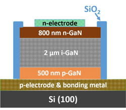
Figure 1: (a) Main steps in fabricating vertical p-i-n diodes on Si; (b, c) As-grown p-i-n diode surface characterized by optical microscopy and atomic force microscopy (AFM); (d) Image of p-i-n epilayers bonded onto Si (100); (e, f) scanning electron microscope (SEM) images of a fabricated p-i-n diode on Si with n-GaN facing up; (g) AFM image of n-GaN surface after AlGaN buffer removal.
The epitaxial material for the fully vertical diodes (Figure 1) was grown on 6-inch (111) Si by metal-organic chemical vapor deposition (MOCVD). The researchers estimated the dislocation density at 9x10⁸/cm2.
Fabrication consisted of etching trenches down to the silicon growth substrate with inductively coupled plasma, depositing and annealing nickel/gold on the p-GaN contact layer, bonding to a (100) Si carrier wafer with copper-tin-copper, removal of the (111) growth substrate by mechanical grinding and plasma etch, plasma-enhanced chemical vapor deposition (PECVD) of silicon dioxide (SiO2) sidewall passivation, removal of the aluminium gallium nitride (AlGaN) buffer, and chromium/gold electrode deposition on the n-GaN contact layer.
The copper-tin-copper bonding step was carried out at 280°C for only 30 seconds to avoid degrading the p-GaN material quality. The researchers also took particular care in etching the AlGaN buffer to limit surface roughness of the n-GaN contact layer to 4.96nm root-mean-square. Rough surfaces lead to increased leakage currents due to electric field spikes.
A 0.11mm2-area device had a forward voltage of 3.35V at 1A/cm2 current density, consistent with the ~3.4eV bandgap of GaN. The resistance was relatively large at low current injection due to the 2μm-thick undoped n--type i-GaN drift region. At higher current injection of 300A/cm2, the forward voltage was 8.38V and the differential resistance was 3.3mΩ-cm2.
The team comments: "The small differential on-resistance of 3.3mΩ-cm2 demonstrated in this work was attributed to conductivity modulation from carrier injection and excellent current spreading in the fully vertical structure."
The researchers also estimate that 1.3V of the 8.38V drop was due to the drift layer with the remainder blamed on contact and series resistance of the p-GaN. Optimizing the p-GaN mobility and ohmic contact metals should reduce the forward voltage and on-resistance.
Under -200V reverse bias, the current was 1x10⁻²A/cm2, which is comparable to other p-i-n diodes on foreign substrates, according to the researchers. The team believes the reverse leakage could be reduced using edge-termination techniques such as sidewall treatment and enhanced passivation. The breakdown voltage was -350V.
"In our diode, when the reverse voltage was larger than 40 V, acceptor traps have been fully ionized and donor traps started to get neutralized," the researchers explain. "As the Fermi level kept moving towards the conduction band, more free electrons were generated in the conduction band, leading to a rapid increase of reverse current."
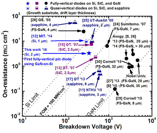
Figure 2: Relationship between specific on-resistance and breakdown voltage of GaN vertical p-i-n rectifiers on various substrates.
The Baliga figure of merit for the device was 37.0MW/cm2 (350Vx350V/3.3mΩ-cm2). The researchers compare this with values obtained on other substrates (Figure 2) and comment: "To our knowledge, this is the best reported data for GaN p-i-n rectifiers grown on Si substrates. Considering the simple active GaN epi-layers with a drift region of only 2μm that can be grown on large-area Si substrates, the methods reported here showed great potential in achieving cost-effective GaN vertical devices for high-power and high-voltage switching applications."

 Ceramic Substrate")


