Researchers in South Korea have used electrochemical potentiostatic activation (EPA) to alter the hydrogen content in p-type gallium nitride (GaN) layers with a view to improved performance of light-emitting diodes (LEDs) [June Key Lee et al, J. Appl. Phys., vol117, p185702, 2015].
The activation of p-GaN is difficult. Present thermal annealing methods generally release holes from about 10% of the magnesium acceptors used for the doping. Poor hole injection reduces the efficiency of GaN-based LEDs.
The presence of hydrogen is difficult to avoid, particularly in metal-organic chemical vapor deposition (MOCVD) where the organic component of precursor molecules such as trimethyl-gallium (Ga(CH3)3) contain hydrogen. Also, the nitrogen source is typically ammonia (NH3).
The team from Chonnam National University, Korea Photonics Technology Institute (KOPTI) and Chonbuk National University believes that there are two main forms of hydrogen incorporation in p-GaN layers (Figure 1): magnesium-hydrogen (Mg-H) complexes and hydrogen interacting in various ways with nitrogen defects (Ga-H).
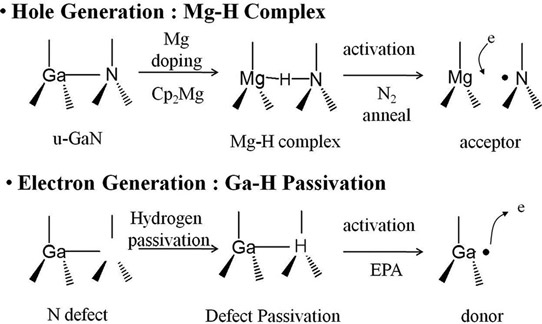
Figure 1: Two types of major hydrogen species inside Mg-doped GaN epilayer. Mg-H complex generates holes if activated, and Ga-H passivation generates electrons if detached.
The Mg-H complexes are believed to form during the cooling process after MOCVD. Removing hydrogen from the Mg-H complexes should release holes, giving improved p-type performance.
The Ga-H family involves nitrogen vacancies that act as electron sources, giving undoped GaN an n-type character. The binding of hydrogen passivates the vacancy, holding the electron in place. Such Ga-H passivation occurs during epitaxial growth.
The electron donor aspect of nitrogen vacancies increases with Mg-doping, compensating hole generation: undoped GaN has electron densities of ~10^{17}/cm3, while Mg-doped GaN has compensating donor densities in the range 1x10¹⁸/cm3-4x1019/cm3.
The activation energy of the donors is less than 100meV, which compares with Mg acceptor activation energies of 170meV. So while many of the donors are activated, only around 10% of the Mg sites are ionized to give free holes.
The Chonnam/KOPTI/Chonbuk team studied simple two-layer and complex LED epitaxial structures. The simple structure consisted of 1μm undoped GaN and 1μm magnesium-doped p-GaN produced on sapphire using MOCVD. LED materials for 385nm ultraviolet and 455nm blue wavelength radiation were also used to create LEDs. These MOCVD materials came from the group's previous work and commercial sources.
EPA for 5 minutes using 1.0M hydrochloric acid electrolyte was found to be more effective in removing hydrogen, compared with a 10 minute anneal at 600°C in nitrogen (Figure 2). Varying the voltage up to 7V gave up to 59% reduction in hydrogen. With 10 minutes of EPA at 5V, the reduction was 63%.
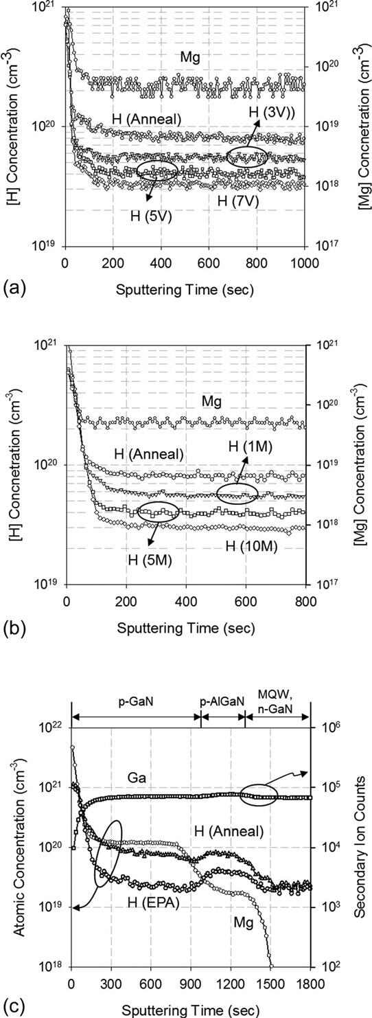
Figure 2: (a) Secondary-ion mass spectrometer (SIMS) depth profile of hydrogen concentration in p-GaN epilayer after 5 minute EPA, and (b) for conventional anneal and 1-, 5-, and 10-minute 5V EPA. (c) SIMS depth profile of hydrogen concentration in 450nm LED epiwafer for conventional anneal and 10-minute 9V EPA.
Performing EPA for 10 minutes at 9V on the 450nm epitaxial wafer reduced the hydrogen content of the p-GaN layer by 70% more than with standard annealing (Figure 2c). The researchers point out that the p-GaN in this case was grown at a low temperature, less than 900°C. Such low-temperature processes are standard, since one does not want to damage the photon-emitting indium gallium nitride (InGaN) multiple quantum wells (MQWs). Standard 700°C annealing processes can remove between 50% and 90% of the hydrogen after 60 minutes.
LEDs with 385nm wavelength increased their output power from 72mW to 86mW at 50mA after 3V EPA for 5 minutes. The reduction in hydrogen content of the p-GaN layer was estimated to be 32%. However, increasing the voltage to 5V reduced the enhancement, giving only 78mW at 50mA. And 7V EPA actually degraded the performance to 67mW, despite a 59% reduction in hydrogen content of the p-GaN layer.
The researchers estimate the internal quantum efficiencies (IQEs) at 67% for 3V EPA, 60% for 5V, and 51% for 7V. Thermally annealed material had an IQE of 55%.
The researchers estimate that the concentration of Ga-H sites in their samples are around 1018/cm3, the same order of magnitude as the hole carrier density. The UV LED results are interpreted as showing that 3V EPA mainly breaks up the Mg-H complexes, while the 7V EPA largely removes the Ga-H passivation. Another research group has determined that 1.93eV is required to break up the Mg-H complex; the Chonnam/KOPTI/Chonbuk team infers from their results that more energy is needed to deactivate the Ga-H passivation.
The researchers comment: "Selective hydrogen elimination from Mg-H complexes is the key to achieving high-quality p-type GaN epi-layers."
EPA experiments on a commercial 450nm LED wafer with ~85% IQE showed no change in IQE, "which indirectly implies that a similar amount of hydrogen atoms was removed from the Mg-H complex and Ga-H passivation", according to the researchers.
The team hopes that further EPA process optimization could lead to lower levels of Mg-doping being needed for a given hole carrier density, which should improve crystal quality and performance of the p-GaN layer in LEDs.
The current-voltage behavior of LEDs with EPA or with annealing were similar above 2V forward voltage. However, in the 1-2V region the 7V EPA was an order of magnitude lower. The reverse-bias behavior was improved with EPA – breakdown was delayed by about 5V and the leakage at 10V was about an order of magnitude lower.
The improved electrical properties also gave increased robustness against external electric stress – the lifetime at 20mA injection was 1000 hours, slightly better than for conventional annealing; electrostatic discharge testing of conventional annealed devices degraded significantly after 3x 1-second 1000V pulses, while EPA LEDs retained their performance characteristics up to 3500V stressing.
 N-Type P-Type Semi-Insulating")