Yellow laser diodes with low thesholds have been produced by Jijun Feng (University of Shanghai for Science and Technology, China) and Ryoichi Akimoto (National Institute of Advanced Industrial Science and Technology (AIST), Japan) based on beryllium zinc cadmium selenide (BeZnCdSe) single quantum well (SQW) light-emitting active regions [Appl. Phys. Express, vol9, p012101, 2016].
The researchers see important potential biomedical applications for yellow (560-590nm) lasers such as flow cytometry and treatment of ocular disorders. Feng and Akimoto recently reported green and green-yellow laser diodes based on BeZnCdSe technology.
Previously groups have developed yellow lasers based on ZnCdSe, but room-temperature operation was only achieved with optical pumping. Although room-temperature operation has been achieved by adding sulfur (ZnCdSSe), the lifetime of devices was low.
Feng and Akimoto's laser heterostructures (Figure 1) were prepared on n-type (001) gallium arsenide (GaAs) using molecular beam epitaxy (MBE). The n- and p-type doping came, respectively, from zinc and nitrogen impurities supplied by zinc chloride and nitrogen activated by radio frequency plasma. Separate chambers were used for II-VI and III-V growth layers. These chambers were connected by an ultra-high-vacuum transfer chamber. The III-V growth consisted of a 500nm n-GaAs buffer.
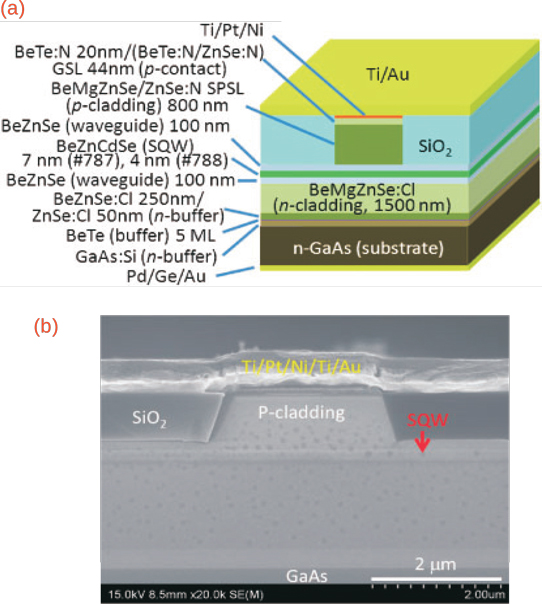
Figure : (a) Schematic diagram of yellow laser diode. (b) Cross-sectional scanning electron microscopy image of fabricated #787 LD (2μm wide).
The laser structure used a separate-confinement heterostructure around the BeZnCdSe SQW. Two samples were produced with SQWs containing varying Cd contents and of different thicknesses – a 7nm well with 47% Cd (#787) and a 4nm well with 52% Cd (#788). The thinner well for #788 avoided cracking of the epilayers. The Be content was around 1% in both cases. The p-side included a short-period superlattice (SPSL) cladding with six-monolayer pairs of BeMgZnSe/ZnSe:N (6ML/6ML). Previous work by a group that included Akimoto used 1000nm BeMgZnSe n-cladding. This was increased to 1500nm to suppress light absorption by the GaAs substrate.
Feng and Akimoto report: "The lattice mismatches for p- and n-cladding layers are about +0.03% to +0.05% and 0.10% to 0.11%, respectively. The use of the SPSL can enhance the p-type doping level of the II–VI cladding layer with a wide bandgap."
Ridge-waveguide lasers were produced by patterned etching 900nm deep. The structure was then covered with 2μm silicon dioxide and polished back with chemical mechanical planarization (CMP). Further etching was performed to expose the metal mask used for the patterned etching. Electrodes were then formed on the p-region and the back-side of the substrate.
The cavities of the devices were formed through cleaving. The facets were coated with silicon dioxide and zirconium dioxide layers to give ~90% reflectivity at both ends of the cavity. The laser diode chips were mounted on copper heat-sinks with indium bonding.
Pulsed lasing above threshold from 500μm-long 5μm-wide laser diodes produced 567nm and 563nm yellow light for samples #787 and #788, respectively. The corresponding full-width at half-maximum (FWHM) values for the peaks were 2.4nm and 1.8nm.
Continuous wave (cw) operation of a 7μm-wide 300μm-long #787 laser diode achieved theshold at 10.8mA and 8.4V. The researchers compare this with a 10μm-wide, 800μm laser diode, previously reported by a group from NAIST and Hitachi in 2011, that achieved threshold at 94mA/9.6V. In terms of current density, Feng and Akimoto's device threshold was 0.51kA/cm2, compared with 1.175kA/cm2 for the 2011 report. The 2011 device used a gain-guided rather than refractive index-guided structure.
Feng and Akimoto attributed the low threshold current density for their laser diodes to suppression of lateral leakage current outside of the electrode by the silicon dioxide insulation around the ridge, confining most of the injected current to a vertical direction. The researchers used a similar approach with their recent green/yellow-green laser diodes.


