KTH-Royal Institute of Technology in Sweden has used corrugated epitaxial lateral overgrowth (CELOG) to create heterojunctions consisting of n-type indium phosphide (n-InP) and p-type silicon (p-Si) [Y. T. Sun et al, Appl. Phys. Lett., vol106, p213504, 2015]. Usually such junctions suffer from high dislocation density due to an 8% lattice mismatch. The CELOG technique allowed KTH to create heterojunction photodiodes (HJPDs).
The researchers comment: "This demonstration of epitaxially grown InP/Si heterojunction photodiodes will open the door for low-cost and high-efficiency solar cells and photonic integration of III-Vs on silicon." They add that CELOG "is a generic technology and can be used to create functional heterojunction structures by integrating various III-V semiconductors on Si substrate."
Monolithic realization of III-Vs on silicon could lead to photonic integrated circuits (PICs), optical interconnects for CMOS electronics, and silicon-based multi-junction solar cells. Although the paper does not mention it, InP is also frequently used as a substrate or buffer layer for the growth of indium gallium arsenide (InGaAs) – a high-mobility channel material that is proposed for integration into future high-speed CMOS electronics.
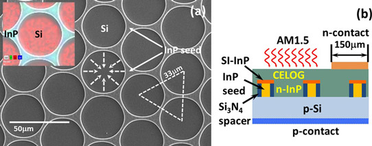
KTH used (001) p-Si substrates offcut 4° in the <111> direction. The processing began with metal-organic vapor phase epitaxy (MOVPE) of 50nm gallium arsenide (GaAs) buffer and 2μm InP seed layers. Then 30μm-diameter circular openings were etched down to the p-Si substrate in a triangular lattice with 33μm center-to-center distance (Figure 1). Wet etching was used to remove residual GaAs in these openings.
Figure 1: (a) Top-view SEM image of engineered seed InP/Si substrate for CELOG with Si surface exposed as circular openings in InP seed layer. Dashed lines indicate directions of growth initiated from surface of seed InP mesa. Inset: SEM/EDS mapping of InP and Si distribution. (b) Schematic cross-section n-InP/p-Si HJPD, not to scale.
The structure was covered with 200nm silicon nitride from plasma-enhanced chemical vapor deposition (PECVD). The silicon nitride was subjected to reactive ion etch with trifluoromethane (CHF3) which, due to its anisotropic action, removed the silicon nitride from the horizontal surfaces of the InP seed layer and the bottoms of the openings.
After cleaning, the CELOG process consisted in 590°C 20mbar low-pressure hydride vapor phase epitaxy (HVPE) of semi-insulating iron-doped InP (5 minutes) and unintentionally doped (UID) n-InP (25 minutes). The sources for the component atoms were indium chloride and phosphine (PH3).
The aim of the semi-insulating InP material was to avoid the formation of shunt paths through the seed material in the fabricated photodiodes. The semi-insulating InP had a resistivity of more than 2x10⁸Ω-cm.
The carrier concentration of n-InP grown on semi-insulating InP substrates is around 1.5x10¹⁵/cm3. The researchers comment: "We chose to use this UID layer of low carrier concentration to form n-InP/p-Si heterojunction due to its higher lateral growth than highly doped n-InP so that a complete coverage of the open circle can be achieved with facility."
Heterojunction photodiodes (HJPDs) were fabricated with gold-germanium/nickel/gold n-InP ohmic contacts and 600nm aluminium ohmic p-contacts on the back-side of the p-Si substrate, thinned to 100μm. The structure was annealed at 380°C for 5 minutes. The 5mmx5mm chips had 25 150μmx150μm n-contact pads, giving around 98% exposed n-InP surface. The n-InP/p-Si regions of the HJPDs had an effective area of 0.185cm2 out of the 0.25cm2 total.
Scanning electron microscope (SEM) studies showed that the lateral growth proceeds downwards from the SI-InP material to cover the silicon surface. Also, triangular voids form between the lateral InP material and the silicon nitride spacer covering the vertical walls of the InP seed material.
The n-InP/p-Si junction has a type-II band alignment where the valence-band and conduction-band energy levels step upwards together from n-InP to p-Si. Such an alignment can be used in photodiodes and photovoltaic cells. The InP has a wider bandgap of 1.35eV, compared with silicon's 1.12eV. Thus, the InP can act as a window layer, filtering out high-energy photons.
The equilibrium depletion region of the pn junction is estimated to be 1.5μm. The built-in electric field in the depletion region will sweep photo-generated electrons and holes into the n-InP and the p-Si regions, respectively, giving a photocurrent. The junction region has an effective indirect bandgap of 0.74eV between the n-InP conduction band and p-Si valence band.
Photoluminescence study of bandgap narrowing suggests a higher impurity concentration of 5.6x10¹⁵/cm3 in the region near the n-InP/p-Si CELOG interface. The researchers attribute the higher concentration to silicon incorporation from the substrate into the InP during CELOG. The PL near the n-InP/p-Si interface is also more intense than that at the CELOG InP surface. The researchers comment: "This is opposite to the conventional direct heteroepitaxial growth of III-V semiconductors on Si, in which the high-density defects accumulate close to the III-V/Si interface and cause low PL intensity."
In fact, the n-InP/p-Si PL was even more intense than that of an n-InP layer grown on an iron-doped InP substrate. The CELOG surface n-InP showed the lowest PL – attributed by the researchers to threading dislocations escaping from the seed region. The dislocation density of the seed was estimated to be ~109/cm2 – a high value.
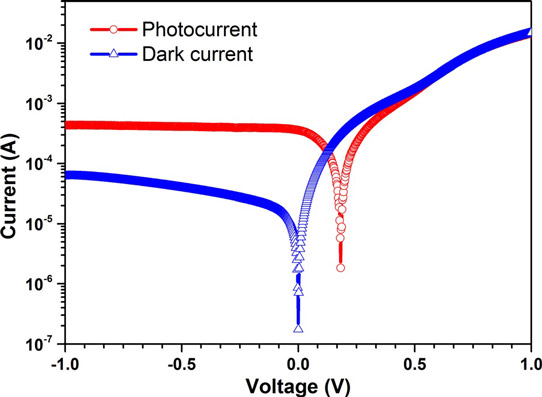
Figure 2: Dark-current and photo-current characteristics of CELOG n-InP/p-Si HJPD in semi-log plot.
The dark current of the HJPD at -1V reverse-bias leakage was 60μA (Figure 2). Expressed as a current density of 0.324mA/cm2, this is much smaller than for wafer-bonded germanium/silicon HJPDs. The photovonltaic effect under AM1.5 solar illumination gave an open-circuit voltage of 180mV and a short-circuit current density of 1.89mA/cm2. The external quantum efficiency (EQE) was estimated at 4.3%. Taking into account the reflection of photons from the InP surface, the internal quantum efficiency (IQE) was 6.4%.
The researchers believe that higher current and efficiencies could be achieved with thinner CELOG InP emitter layers.


