Researchers based in the USA and France have created graphene nanoribbon structures with regions that have relatively large energy bandgaps of about 0.5eV [J. Hicks et al, Nature Physics, published online 18 November 2012].
Flat graphene tends to have a zero/minimal gap, with the energy bands meeting in a 'Dirac cone' at six 'Dirac points' in wavevector (k) space.
Materials with zero bandgap have (semi-)metallic behavior for electron flow. This is attractive for interconnects, but not if one wants active switching or amplification. For active devices one needs materials with controllable bandgaps. Imperfections in graphene produced by lithography techniques can widen the bandgap, but not in a controllable manner.
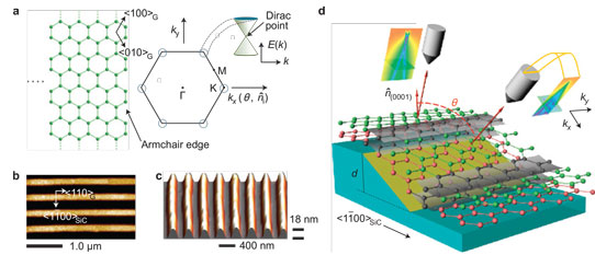
Figure 1: Experimental geometry of graphene on SiC trenches: a, graphene Brillouin zone orientation relative to armchair edge ribbons; b, AFM top view of sidewall ribbons showing long-range order; c, perspective AFM view of 18nm-deep graphitized trenches; d, schematic side-view of sidewall ribbons containing two graphene sheets (lower sheet in red is referred to as buffer). Grey regions are curved semiconducting parts of the graphene structure. Schematic shows two detector orientations used to reach both the K-point (Dirac point) of flat surface and facet.
The behavior of electrons near the Dirac points can be approximated with a two-dimensional Dirac equation. The Dirac equation is the relativistic generalization of the Schrodinger equation that describes the spin-1/2 behavior of electrons, neutrinos and quarks. For these particles the energy–wavevector relation is cone-like if they have negligible rest mass (m0, the mass of the stationary particle) – i.e. the energy is very much greater than m0c2.
The work of creating and measuring the 0.5eV bandgap of graphene nanoribbons was carried out at the USA's Georgia Institute of Technology, along with scientists from France's CNRS, Cassiopée beamline (SOLEIL), Institut Jean Lamour in Nancy and Institut Néel in Grenoble.
Georgia Institute of Technology has previously worked with Institut Néel on using bottom-up techniques to grow graphene nanoribbons on silicon carbide (SiC) with bandgaps. In 2010, they reported graphene nanoribbons with small bandgaps by growing them along steps in the SiC surface. The bending of the graphene introduces strain and hence a bandgap. The strain can be controlled by varying the step height. Also, confinement effects are believed to play a role in developing the bandgap in nanoribbons.
The new structures build on this work and were produced on n-type 4H-SiC substrates. Vertical trenches were produced in the (0001) surface by reactive ion etch (RIE) and then graphitized to create graphene bilayers. The 1mm-long trenches were between 7.5nm and 18nm deep and were arranged in an array with a pitch of 400nm over a 1mm x 3mm area. The graphitization was carried out in a carbon radio-frequency furnace at a temperature of 1560°C. The initially vertical walls of the SiC surface become facets during the graphene growth process. The ribbons were up to 36nm wide.
The main technique used to explore the band structure of the resulting material was angle-resolved photoemission spectroscopy (ARPES), where x-rays are used to eject electrons whose angle and energy are measured to give information about their original state in the material.
The ARPES measurements were carried out at the Cassiopée beamline at the SOLEIL synchrotron facility in France. The samples were transported in air to the SOLEIL site. The samples were annealed at 800°C in ultra-high vacuum before the ARPES measurements were made at 100K.
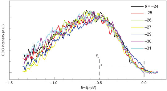
Figure 2: Normalized energy distribution curves (EDCs) of cones in the transition region for different angles. All cones in the transition region have the same profile, demonstrating the 1D nature of the region.
The bandgap for 1.4nm bent sections of graphene nanoribbon was found to be more than 0.5eV. This determination is based on the top of the valence band being measured at –0.5eV relative to the Fermi level (Figure 2). Since the bottom of the conduction band is not observed, it must be above the Fermi level. The flat sections had traditional metallic properties with zero bandgap. The flat regions were n-type (negative charge electron conductivity) and the bent regions were p-type (positive charge hole conductivity).
"We can make thousands of these trenches, and we can make them anywhere we want on the wafer," said Georgia Institute of Technology professor Edward Conrad. "This is more than just semiconducting graphene. The material at the bends is semiconducting, and it's attached to graphene continuously on both sides. It's basically a Schottky barrier junction."


