Germany-based researchers claim a record on-current for an enhancement-mode (e-mode) gallium nitride (GaN) metal insulator semiconductor heterostructure field-effect transistor (MISHFET) on silicon (Si) substrate [Herwig Hahn et al, Jpn. J. Appl. Phys., vol52, p090204, 2013].
Nitride semiconductor transistors are being developed for high-power and high-frequency applications. Producing such devices on silicon would reduce material costs and introduce economies of scale from the larger substrates available (up to 300mm).
Another desirable characteristic is enhancement-mode operation rather than the depletion-mode operation that is usual with nitride semiconductor transistors. Enhancement-mode transistors are in the off-state at zero gate potential, reducing power consumption. Further, e-mode operation is important for fail-safe power circuits.
There are a number of techniques to shift the threshold voltage of nitride semiconductor transistors to positive e-mode values. The team from RWTH Aachen University, Fraunhofer IAF and Aixtron used gate recessing, reducing the thickness of the aluminium gallium nitride (AlGaN) barrier, to achieve this. In addition, a gate insulator material, aluminium oxide (Al2O3), was applied to reduce gate leakage currents through the barrier.
The epitaxial structure for the transistors (Figure 1) was produced up to the GaN cap on 6-inch (150mm) silicon using metal-organic chemical vapor deposition (MOCVD). A thin 1.5nm AlN layer above the GaN buffer has been found to enhance mobility in the two-dimensional electron gas (2DEG) used as the transistor channel.
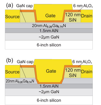
Figure 1: Schematic cross sections of unrecessed (a) and deepest recessed (b) devices.
The material was diced into 15mm x 15mm pieces. The first fabrication steps consisted of dry etch mesa isolation and the application and annealing of titanium/aluminium/nickel/gold ohmic source-drain contacts. After a 120nm silicon nitride (SiN) passivation, the pieces had a sheet resistance of 280Ω/square and a two-dimensional electron gas mobility of 2100cm2/V-s.
Gate recessing was achieved by opening a trench with a soft fluorine-based dry etch and continuing into the AlGaN barrier with a chlorine-based digital dry etch. Digital etching refers to a precise layer-by-layer removal that is rather similar to atomic layer deposition (ALD) in reverse. The depth of the digital etch was varied, leaving differing thicknesses of AlGaN barrier under the gate.
Gate stack formation was completed with atomic layer deposition of Al2O3 insulation, and electron-beam evaporation of platinum/gold electrodes.
Capacitance-voltage (C-V) measurements allowed estimation of the barrier thicknesses for the four samples produced: 22nm (no digital etch), 8.8nm, 5.1nm, and 2.1nm. The last sample barrier thickness suggests that the majority is made up of the 1.5nm AlN layer. The C-V analysis also suggests a positive threshold and near zero hysteresis for the 2.1nm barrier. However, stressing the sample to more negative voltages of -6V does give a hysteresis effect of 100mV, comparable to that found with the other samples.
Direct current measurements (Table 1) were made to determine threshold voltage (Vth), maximum drain current (Id,max), maximum transconductance (gm,max), source resistance (Rs), and intrinsic maximum transconductance (gim,max) for devices with 1μm gate length.
Table 1: Extracted DC values for all samples.
Barrier thickness Vth Id,max gm,max Rs gim,max 22nm -3.83V 1.36A/mm 215mS/mm 2.14Ω-mm 400mS/mm 8.8nm -1.22V 1.16A/mm 260mS/mm 2.08Ω-mm 566mS/mm 5.1nm +0.00V 1.27A/mm 342mS/mm 1.97Ω-mm 1050mS/mm 2.1nm +0.82V 1.35A/mm 366mS/mm 1.95Ω-mm 1280mS/mm
The enhancement-mode device with positive threshold voltage (2.1nm barrier) has maximum drain current of 1.35A/mm: "the highest value reported so far when a silicon substrate is used", according to the research team. Although shorter gates should theoretically lead to higher drain currents, the researchers warn that the threshold voltage would also be expected to shift.
The transconductance measurement was affected by the relatively high contact resistance, as shown by the intrinsic transconductance being up to a factor of four higher. The researchers believe that optimizing the contacts to give a contact resistance of 0.3Ω-mm could boost transconductance to 0.7S/mm (700mS/mm). The contact resistance of the measured devices was estimated at 1.75Ω-mm.
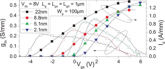
Figure 2: Drain current (Id) and transconductance (gm) characteristics for all four samples.
The subthreshold swing values were in the range 80-100mV/dec. With 8V drain bias, the gate leakage current under negative gate potential was as low as 10nA/mm. This would enable devices with on-off ratios of the order of 108. However, setting the off condition to that of 0V gate for enhancement-mode operation gives a 'real' on-off ratio of 104.
The gate leakage increases with positive gate potentials, with the thinner barriers naturally offering less resistance to current flow. Even so, the leakage is less than 1mA/mm for the on-current of 1.3A/mm in the 2.1nm barrier device.
The researchers comment: "The values are below the ones reported in literature for e-mode metal insulator semiconductor heterostructure field effect transistors (MISHFETs) and much better than those for Schottky-gated e-mode devices." The maximum applicable extrinsic gate potential of +7V is limited by dielectric breakdown.
Three-terminal measurements at 0V gate gave a breakdown voltage of around 65V drain for the 2.1nm barrier device with 2μm gate length and a gate-drain spacing of 2.5μm. The "rather early breakdown" is blamed on the aluminium oxide in the absence of an exponential behaviour that would indicate buffer problems.
Pulsed measurements to assess current collapse effects were also carried out on devices with a 2.1nm barrier. The researchers compared the specific on-resistance (RonxA) at 65% maximum current for a pulsed unbiased state that eliminates thermal effects and for a 50V drain bias to reveal current collapse. In the thin 2.1nm barrier device (1.5μm gate-source, 1μm gate, 2.5μm gate-drain, 100μm width), the unbiased specific on-resistance was 0.24Ω-cm2, which increased by 20% to the biased/current collapse value of 0.29Ω-cm2. By contrast, the non-recessed/22nm barrier device showed a 70% increase in on-resistance in the bias/current collapse mode.
The researchers comment: "We believe that the suppression of the current collapse (even if not as good as for a comparable HFET) is related to the slanted gate shape in combination with a barrier recess which reduces trapping phenomena by the passivation/barrier interface."
In the future, it is believed that the threshold voltage could be shifted to even more positive values by fluorine implantation or by adding a back-barrier.


