An international team of researchers has been exploring nanomembranes of beta-phase gallium oxide (β-Ga2O3) as a channel material for high-voltage field-effect transistors (FETs) [Wan Sik Hwang et al, Appl. Phys. Lett., vol104, p203111, 2014]. The researchers are variously associated with Korea Aerospace University, University of Notre Dame, USA, University of California Santa Barbara, USA, IBM T. J. Watson Research Center, USA, Leibniz Institute for Crystal Growth, Germany, and University of Parma, Italy.
Bulk β-Ga2O3 has a wide bandgap energy of around 4.9eV, which should correspond to high critical fields for breakdown. This bandgap is even wider than those for materials such as silicon carbide (SiC ~3.3eV) or gallium nitride (GaN ~3.4eV) that are presently being developed for high-voltage and high-power applications.
The drawback of β-Ga2O3 for such applications is a low thermal conductivity of 13W/m-K, compared with 150W/m-K for Si, 150?200W/m-K for GaN, and 360-400W/m-K for SiC. For power devices, thermal management requires high thermal conductivities to enable efficient heat dissipation.
The research team believes that thin layers of β-Ga2O3 integrated with more thermally conductive substrates could overcome the heat dissipation problem. Such integration has been demonstrated for low-power electronics based on layered materials such as graphene and metal dichalcogenides such as molybdenum disulfide (MoS2).
The researchers used a mechanical exfoliation technique to create nanomembranes of β-Ga2O3. Mechanical exfoliation with sticky tape applied to graphite is how graphene was first produced for characterization.
Although β-Ga2O3 does not have the layered structure of graphene that has strong in-plane covalent bonds and weak intra-plane van der Waals bonding, mechanical exfoliation nevertheless results in nanomembranes of thickness between 20nm and 100nm. The researchers suggest that, despite β-Ga2O3 technically being a three-dimensional crystal (Figure 1), the long lattice constant in the (100) direction (a) leads to easier exfoliation than expected.
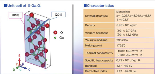
Figure 1: Crystal structure and properties from http://www.mtixtl.com/Ga2O3onAl2O3-101005S1-1.aspx
The researchers admit: "Mechanical exfoliation is indeed not a scalable method, but methods similar to smart-cut technology used in silicon-on-insulator (SOI) wafer manufacture can potentially enable controlled release of large nanomembranes of the wide-bandgap material. Such a method can potentially enable the integration of nanomembrane high-voltage transistors on multiple platforms for high-voltage switching and power management."
The 20mm-diameter single crystals of β-Ga2O3 were produced by the Czochralski process of slowly drawing the crystal out of a melt in an iridium crucible. The melting point of β-Ga2O3 is 1820°C. The crystal growth was carried out in a dynamically adjusted atmosphere designed to reduce decomposition of the Ga2O3 while avoiding oxidation of the iridium crucible.
The researchers produced 1cm-side cubes of β-Ga2O3 crystal with exposed (100) planes for exfoliation and easy cleaving. Hall measurements in the Van der Pauw configuration with indium/gallium contacts gave a free-electron concentration of 5.5x10¹⁷/cm3, mobility of 112cm2/V-s, and resistivity of 0.1Ω-cm.
Energy-dispersive x-ray analysis gave an optical bandgap of 4.77eV for the nanomembrane material. Band-structure calculations suggest an indirect bandgap of 4.85eV, with a slightly larger direct gap of 4.88eV at the Γ-point (k=0). The conduction-band minimum is at Γ with an almost isotropic effective mass of 0.28x the free-space mass. The valence-band maximum is located along the I-L line.
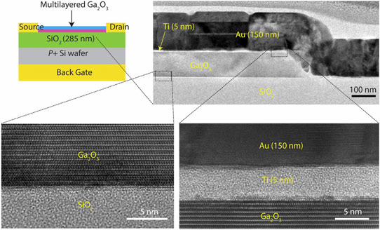
Figure 2: Cross-sectional TEM image of β-Ga2O3 FETs, showing a flat interface between β-Ga2O3 and the SiO2 dielectrics as well as between the β-Ga2O3 and the Ti/Au electrode.
The transistor structure (Figure 2) used a back-gate. The exfoliated Ga2O3 nanomembrane was transferred to a thermal silicon dioxide layer on a silicon substrate. The source/drain electrodes consisted of titanium/gold annealed at 300°C for three hours in an argon/hydrogen environment. Transmission electron micrography (TEM) was used to confirm that the lattice parameters of the nanomembrane were unchanged from the bulk values "indicating minimal strain and damage in the transfer and device fabrication process". In particular, the material was unstrained in the channel, under the source/drain contacts, and at the interface with the underlying silicon dioxide.
With a high 20V drain bias, the gate was able to modulate the current by a factor of ~107 at room temperature. The limiting factor for the on/off current range was not the channel, but rather gate leakage. The extrinsic field-effect mobility (uncorrected for contact resistance of ~55Ω-mm) was 70cm2/V-s. The real 'intrinsic' mobility of the device is expected to be nearer the bulk value at ~130cm2/V-s.
Although the subthreshold swing of 200mV/decade is far from the ideal 60mV/decade, the researchers comment that the value is "encouraging", given the unoptimized interfaces and the thick silicon dioxide back-gate dielectric layer. The device has an unintentional n-type (negative electron charge carriers) behavior. This could be due to atomic defects and/or impurities.
The researchers believe that the relatively high contact resistance could be improved by using metals with low workfunction or by ion implantation of dopants under the contacts. The present contact resistance performance is comparable to that obtained with MoS2 transistors. While MoS2 transistors tend to suffer avalanche breakdown at around 15V (Figure 3), Ga2O3 transistors "maintain a robust current saturation up to 70V with no signs of output conductance".
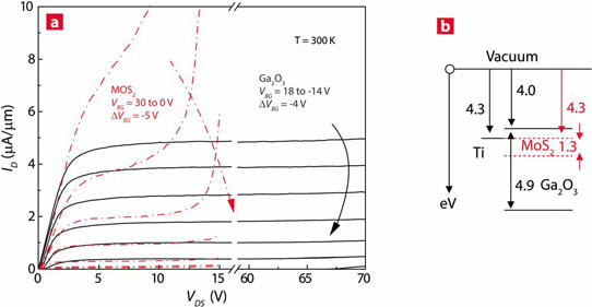
Figure 3: (a) Common-source transistor characteristics, drain current versus drain bias in linear region and current saturation under high drain bias, and comparison of breakdown voltage of β-Ga2O3 and MoS2. Device widths/lengths of 1/3μm. (b) Band diagram of β-Ga2O3 compared with MoS2, indicating formation of Schottky barrier contact between metal and β-Ga2O3.
The researchers add: "This result shows that nanomembrane β-Ga2O3 channel transistors can sustain and switch high voltages even when integrated in thin layer forms on foreign substrates. High thermal conductivity but electrically insulating layers such as AlN or BN can be used to help circumvent the low thermal conductivity of the β-Ga2O3 channel. The high-thermal-conductivity insulating layers can also serve as the gate insulator for the transistor."


