Singapore researchers report "for the first time" the DC and microwave characteristics of submicron-gate aluminium gallium nitride on gallium nitride (AlGaN/GaN) high-electron-mobility transistors (HEMTs) on 8-inch (200mm) diameter Si(111) substrate [Subramaniam Arulkumaran et al, Jpn. J. Appl. Phys., vol51, p111001, 2012]. The researchers are at Nanyang Technological University, Institute of Materials Research and Engineering, and Institute of Microelectronics.
"Our results show the feasibility of achieving device-quality AlGaN/GaN HEMT structure on 8-inch diameter Si(111) for low-cost high-frequency and high-power switching applications," the researchers write.
Nitride semiconductor devices have been recently developed for high-frequency and switching power applications, based on these materials' high saturation velocity at high electric field, high breakdown electric field, and high electron mobility.
The development of nitride semiconductor transistors on silicon substrates is widely seen as a way to lower production costs through using less expensive material and through economies of scale. In particular, silicon is much less expensive than silicon carbide (SiC) and, further, is available in larger-diameter substrates.
Although sapphire is lower cost than silicon carbide and is more established for growing nitride semiconductors for LEDs, it is a poor thermal conductor, making it less attractive for power applications.
AlGaN/GaN HEMTs grown on 200mm substrates are particularly attractive since there are many 200mm silicon facilities that are underutilized with the transition to 300mm production (and 450mm being actively developed for the future).
Of course, there are challenges of growing nitrides on larger-diameter wafers, such as bowing of the substrate and resulting non-uniform material qualities.
The Singapore epitaxial material (Figure 1) was grown in a Veeco TurboDisk k465i metal-organic chemical vapor deposition (MOCVD) system. The substrate resistivity was ~40Ω-cm. The epitaxial material had mobility and sheet carrier concentrations of 1550cm2/V-s and 0.84x10¹³/cm2, averaged over five samples. The average sheet resistance was less than 400Ω/square.
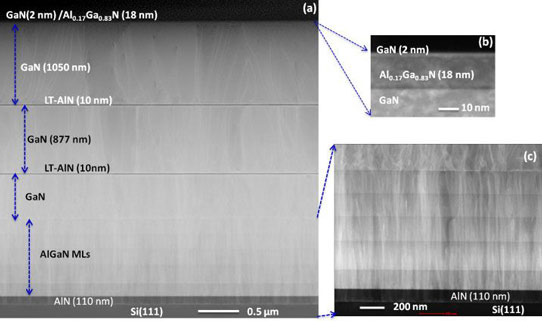
Figure 1: (a) Typical cross-sectional high-angle annular dark-field scanning transmission electron microscopy (HAADF-STEM) image of the full HEMT structure on 8-inch diameter Si(111) substrate. (b) HAADF-STEM z-contract image of the same sample showing GaN cap layer and AlGaN barrier layer (c) HAADF-STEM z-contrast image of the same sample showing stress mitigation layers [AlGaN multi layers (MLs) on a 110 nm-thick AlN nucleation layer] on 8-inch Si(111).
The epitaxial material was diced into small pieces before transistor processing. Mesa isolation was achieved through inductively coupled plasma etch. The ohmic contacts were titanium/aluminium/nickel/gold with a contact resistance of 1.8Ω-mm. Mushroom-shaped Schottky gates were formed using nickel/gold with a source-gate distance of 0.8μm, gate width of 2x25μm, gate length (Lg) of 0.3μm, and gate-drain distance (Lgd) of 1.25μm. The gates of separate transistors were separated by 12μm.
The maximum drain current was 853mA/mm. The peak intrinsic transconductance of 180mS/mm occurred at -2.3V gate potential and 10V drain bias. The threshold voltage was -3.8V.
Microwave performance was tested on 0.3μm gate-length devices with 2μm Lgd and 2x75μm gate width. The unit current gain cut-off frequency (fT) was 28GHz and the maximum oscillation frequency (fmax) was 64GHz, for 10V drain and -2.4V gate. The cut-off-gate-length product (fTxLg) was 8.4GHz-μm, a value comparable with that achieved on smaller-diameter silicon substrates.
The researchers comment: "The observed fmax/fT > 2 to 2.66 is due to the occurrence of good-quality buffer GaN with low buffer leakage current (4.8x10⁻³mA/mm at 100V)."
At a bias of 100V, the on/off ratio was 1.36x10⁵, according to channel and buffer-leakage current measurements. Devices with 0.3μm gate length (Lg) and 2μm gate-drain separation (Lgd) showed gate-drain breakdown (BVgd) of 60V with a 0.5mA/mm current. Devices with 2μm gate length and 6μm gate-drain separation had increased breakdown performance, with BVgd at 188V. Buffer breakdown occurred in the long-gate device at 192V. A rough indication of the breakdown field is given by BVgd/Lgd, which is ~0.3MV/cm for both devices.
The researchers see the breakdown performance as being limited by GaN buffer thickness and crystalline quality.


 Cylinder Gas Tungsten Hexafluoride")

