02 Aug 2012 German company will lead a new effort to shrink extreme ultraviolet (EUV) lithography resolution from 20nm to 14nm.

EUV optics
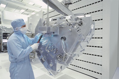
The optics giant Carl Zeiss is to lead a new project to improve the resolution of extreme ultraviolet (EUV) optics well beyond what will be possible with the first generation of production systems.
ASML’s first EUV lithography tools, scheduled to ship to customers early next year and go into full semiconductor wafer production in 2014, will be able to manufacture structures as small as 20nm.
But the semiconductor industry's roadmap calls for even smaller structures than that in the future, and the objective of the Zeiss-led project is to extend EUV resolution to just 14nm.
Funded by the German Ministry of Education and Research (BMBF), the three-year, €7million “ETIK” project is focused on the optical elements of EUV systems, including a new design for the surface of the mirrors used in the projection lens.
Collaboration
Working alongside Zeiss on the project are six other companies and institutes in Germany. They include Berlin-based Bestec, which is developing a new generation of reflectometers to measure the reflectivity of the EUV optics, and IMS CHIPS in Stuttgart, which will provide optical components for the projection lens.
Also involved are The Institute for Technical Optics at Stuttgart University, as well as the Fraunhofer institutes for Electron Beam and Plasma Technology in Dresden, for Applied Optics and Precision Engineering in Jena, and for Material and Beam Technology, also in Dresden.
In a statement, Andreas Dorsel from Carl Zeiss Semiconductor Manufacturing Technology commented: “We see EUV technology as the key to the microelectronics of tomorrow. The project unites proven experts who will now take EUV to the next level.”
Although the principles behind EUV lithography – using 13.5nm light to pattern semiconductor wafers with unprecedented precision - have long been understood, the technology is only just becoming viable for the commercial world.
The major stumbling block has been the output power and stability of the EUV light source, but with laser-driven sources now starting to reach power levels that are high enough to support the productivity of a modern semiconductor chip fab, plus the promise of heavy investment in future tool development from Intel, it appears that the era of EUV lithography is finally about to dawn.


