Nanometer-scale silicon crystals have been shown to generate high luminous potential, and scientists at Karlsruhe Institute of Technology (KIT) in Germany and the University of Toronto in Canada have succeeded in using these crystals to manufacture silicon-based light-emitting diodes (SiLEDs). The researchers say that the SiLEDs are free of heavy metals and can emit light across a range of wavelengths (published in Nano Letters journal - DOI: 10.1021/nl3038689, February 2013).
Generally, silicon is considered to dominate as the material of choice for semiconductors in microelectronics and photovoltaics applications, but for a long time it has been considered to be unsuitable for LEDs. However, this is no longer true for particles of nanoscopic dimensions, since silicon nanocrystals have been shown to produce light.

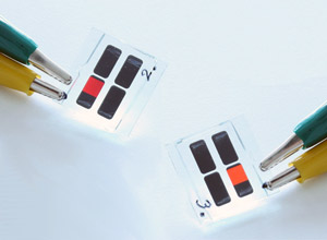
Picture: Liquid-processed SiLEDs: by changing the silicon nanocrystal size, the light emission color can be varied. (Photo: F. Maier-Flaig, KIT/LTI)
The nanocrystals consist of a few hundred to thousand atoms and are showing considerable potential as highly efficient light emitters, according to professors Uli Lemmer and Annie Powell at KIT and professor Geoffrey Ozin at Toronto. In a joint project, the scientists have now succeeded in manufacturing highly efficient SiLEDs from the silicon nanocrystals.
So far, manufacturing has been limited to silicon LEDs emitting light in the red visible spectral range and the near infrared. Regarding the efficiency of silicon LEDs emitting red light, the Karlsruhe researchers say that they are “already leading the world”. “Controlled manufacture of diodes emitting multi-color light, however, is an absolutely novelty,” says Florian Maier-Flaig, a scientist at KIT ‘s Light Technology Institute (LTI) and a doctoral student in the Karlsruhe School of Optics and Photonics (KSOP). The KIT researchers alter the color of the light emitted by the diodes by separating the nanoparticles by their size.
“Our light-emitting diodes have a surprising long-term stability that has not been achieved before,” adds Maier-Flaig. The increased operational lifetime of the components in operation is due to the use of nanoparticles of one size only. This enhances the stability of the sensitive thin-film components. Short circuits due to oversized particles are avoided.
The development made by the researchers at Karlsruhe and Toronto is also characterized by an impressive homogeneity in the luminous areas. The KIT researchers are among the few teams in the world that know how to manufacture such devices, it is claimed.
“With the liquid-processed silicon LEDs that may potentially be produced on large areas as well as at low costs, the nanoparticle community enters new territory, the associated potentials of which can hardly be estimated today. But presumably, textbooks about semiconductor components have to be rewritten,” says Geoffrey Ozin, who is currently a KIT distinguished research fellow at KIT’s Center for Functional Nanostructures.
The SiLEDs also have the advantage of not containing any heavy metals. In contrast to cadmium selenide (CdSe), cadmium sulfide (CdS) or lead sulfide (PbS) used by other groups of researchers, the silicon used by this group for the light-emitting nanoparticles is not toxic. Moreover, silicon is available at a relatively low cost and is highly abundant on earth. Due to their many advantages, the SiLEDs will be developed further in cooperation with other partners, say the researchers.

