Hong Kong University of Science and Technology has achieved record maximum drain currents and peak transconductances for enhancement-mode(normally off)metal–oxide–(nitride)semiconductor heterojunction field-effect transistors(MOSHFETs)on silicon substrates[Tongde Huang et al,IEEE Electron Device Letters,published online 21 June 2012].
The researchers used aluminium nitride(AlN)barriers on gallium nitride(GaN)buffer layers,giving high values for carrier density in the two-dimensional electron gas(2DEG)channel due to the high spontaneous polarization field of the barrier.This reduces on-resistance.
The source and drain regions consisted of re-grown GaN that was heavily doped,reducing access resistance and thus also improving performance.Nitride semiconductor transistors often have source–drain contacts applied directly to the barrier layer,which creates high access resistance.
Researchers are seeking low-cost production of nitride semiconductor devices through growth on large-diameter silicon substrates.It is hoped such devices will be able to handle higher power densities,voltages and frequencies for radio-frequency transmission amplification and for power switching in voltage conversion equipment.A further requirement is for normally-off behavior,reducing power consumption and giving simpler circuits,which can be difficult to achieve in nitride transistors.
The nitride semiconductor heterostructure was grown on 2-inch high-resistivity(HR,resistivity>5000Ω-cm)silicon(111)using metal-organic chemical vapor deposition(MOCVD).The growth began with 40nm of AlN nucleation,eight periods of AlN/magnesium-doped GaN(Mg:GaN)(11nm/23nm)strain relaxation superlattice,two cycles of GaN/low-temperature AlN(600nm/20nm),and 125nm Mg:GaN.The structure was completed with a 875nm GaN buffer,1.5nm AlN barrier,and 1nm GaN protective cap.
The mask for the re-growth step consisted of 84nm of silicon dioxide applied using plasma-enhanced chemical vapor deposition(PECVD).The mask was patterned using a dilute hydrofluoric wet etch.Chlorine-based plasma etch was used to etch out the source–drain regions to a depth of 120nm.
Silicon-doped GaN was re-grown in the source–drain regions using MOCVD at 1090°C.The doping was stepped with a more lightly doped region(2.5x10¹⁹Si/cm3)designed to provide a transition between the pure GaN of the buffer and the highly doped(6x10¹⁹Si/cm3)surface.The aim was to improve surface quality.
After removal of the mask,the gate stack was applied,consisting of 6nm of aluminum oxide(Al2O3)dielectric and nickel/gold metal.The dielectric was applied using atomic layer deposition(ALD)at 300°C.A further 20nm of Al2O3 was applied as passivation after the gate metal.The samples were then subjected to annealing at 400°C for 10 minutes to enable gate sinking.
The metal contacts for the source–drain regions consisted of non-alloyed titanium/aluminum/nickel/gold.These were deposited after Al2O3 removal from the source–drain regions using hydrofluoric acid.The source–drain contacts were deposited last to avoid the thermal anneal.
Two MOSFET types were produced(Figure 1).MOS1 had a 1.3μm gate length and 3μm source–drain distance.For MOS2,the gate length and source–drain distance were the same at 0.7μm.
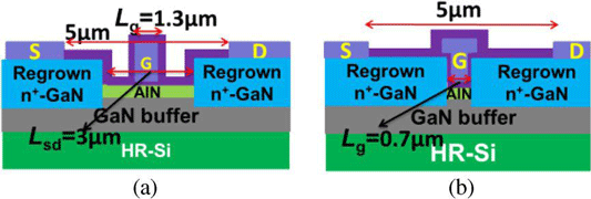
Figure 1:Device schematics of(a)MOS1 with gate length of 1.3μm and source–drain spacing of 3μm,and(b)MOS2 with gate length of 0.7μm.
The maximum drain current at gate potential+2V was 580mA/mm for MOS1 and 860mA/mm for MOS2.Pulsing the gate potential for 500μs showed current collapse for MOS2,but not significantly for MOS1."The more severe current degradation in MOS2 is due to the higher electric field at the drain edge when compared with the case of MOS1,"the researchers comment.
The peak transconductances for 4V drain bias were 324mS/mm and 509mS/mm for MOS1 and MOS2,respectively.The drain current and peak transconductance values are the highest for enhancement-mode(E-mode)MOSHFETs or HFETs on Si,according to the researchers'knowledge(Figure 2).
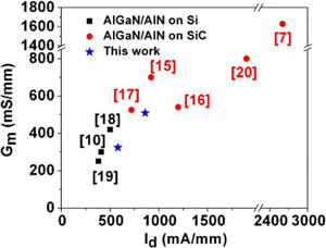
Figure 2:Comparison of peak transconductance as a function of maximum drain current value of GaN HEMTs on Si and GaN HEMTs on SiC(references available in paper).
The researchers believe that reducing the gate length could improve the performance to be comparable with that of devices produced on much more expensive silicon carbide(SiC)substrates.
The threshold voltages are estimated to be+0.15V for MOS1 and+0.21V for MOS2.The respective on-resistance values(+2V gate)are 2.83Ω-mm and 1.63Ω-mm,respectively.The better transconductance of MOS2 can be explained as being due to its lower source access resistance.
At 4V drain bias,the on–off ratio is about 106 between the gate potentials+2V and-0.5V for both transistor types.The gate leakage is smaller than 10-3mA/mm.
The off-state(-0.5V gate)three-terminal breakdown in MOS1 occurs at 62V drain bias due to an increase in buffer leakage.Thus,an improvement in buffer could benefit the breakdown performance of MOS1.
The MOS2 breakdown occurs around 5.8V due to breakdown in the Al2O3 dielectric in the overlapping region between the gate and drain re-growth region."The breakdown voltage of MOS2 could be increased by asymmetric re-growth technology with a large gate/drain spacing,"the researchers believe.